 Products Home / Actuators, Adjusters, & Transducers / Piezoelectric Chips and Stacks / Single-Crystal Piezo Chips and Stacks
Single-Crystal Piezo Chips and Stacks
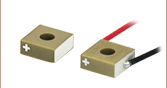
- Single-Crystal Piezo Chips
- Stack Constructed from Multiple Single-Crystal Chips
- Highly Linear Motion with Low Hysteresis
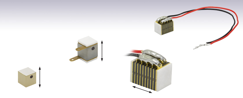
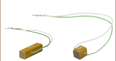
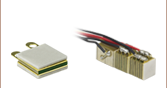
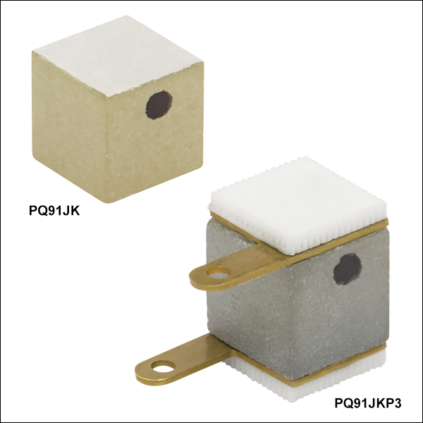
PQ91JKP3
Chip with Copper Top and Bottom Electrodes
PQ91JK
Chip with Bare Top and Bottom Electrodes
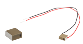
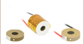
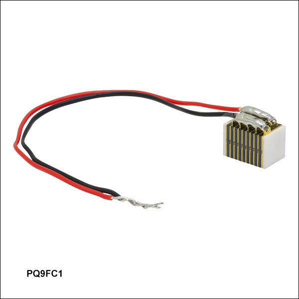
PQ9FC1
Stack with Wire Leads
The wire leads on the PQ9FC1 piezo stack are approximately 75 mm long.
Arrows Indicate Direction of Expansion


Please Wait
| Table 1.1 Piezo Selection Guide |
|---|
| Piezoelectric Ceramic Chips |
| Square |
| Square with Through Hole |
| Round |
| Ring |
| Tube |
| Shear |
| Benders |
| Single-Crystal Piezoelectric Chips |
| Square |
| Piezoelectric Ceramic Stacks |
| Discrete, Square |
| Discrete, Square with Through Hole |
| Discrete, Round |
| Discrete, Ring |
| Discrete, Hermetically Sealed |
| Discrete, Shear (1D to 3D Positioners) |
| Co-Fired: Square, Square with Through Hole, Round, & Ring |
| Co-Fired or Discrete: Square with Strain Gauges |
| Piezoelectric Crystal Stacks |
| Square |
| Mounted Piezoelectric Actuators |
| Ultrasonic Piezo Chips & Transducers |
| Vibrating Piezo Actuator |
| Webpage Features | |
|---|---|
| Clicking this icon below will open a window that contains item specific specifications and mechanical drawings. | |

Features
- <3% Hysteresis at 25 °C Over Full Travel
- Single-Crystal Chips:
- Mounting Face Dimensions: 3.0 mm x 3.0 mm
- Drive Voltage Range: 0 to 1000 V
- Recommended Load of 24 N (5 lbs)
- Bare Electrodes or Copper Foil Leads
- Discrete Crystal Stack:
- Mounting Face Dimensions: 5.0 mm x 5.0 mm
- Drive Voltage Range: 0 to 500 V
- Recommended Load of 64 N (14 lbs)
- Lead Wires
- For Use in Open-Loop Setups
- End Hemispheres and Flat End Plates also Available Separately
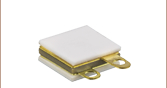
Thorlabs' Single-Piezoelectric-Crystal Chips and Piezoelectric-Crystal Stacks are fabricated from lead-based crystals that exhibit highly linear movement with low hysteresis and creep, making these devices well-suited for open loop applications or operation without position control. Electrodes are printed on the top and bottom of each crystal. Single-crystal chips are offered with bare electrodes or with pre-attached copper foil leads. The discrete stack consists of multiple single-crystal chips and copper plates bonded together with epoxy, with wire leads linking the electrodes in the stack. The PQ91JKP3 chip and PQ9FC1 stack come with pre-attached flat ceramic end plates.
The maximum displacement of these actuators is achieved when they are preloaded with the maximum displacement load, which is specified below for each product. The actual value of the maximum displacement varies for each item and must be experimentally determined; however, the maximum displacement will always be larger than the free stroke displacement. Please see the Operation tab for additional information.
Our single-crystal chips have a drive voltage range of 0 to 1000 V, while our piezo crystal stack has a drive voltage range of 0 - 500 V. A black dot on each chip indicates the positive electrode. Each single-crystal stack has a red wire lead connected to its positive electrode.
Thorlabs' piezoelectric chips are individually inspected using a proprietary AI algorithm to ensure the highest quality of our line of piezo chips, actuators, and transducers.
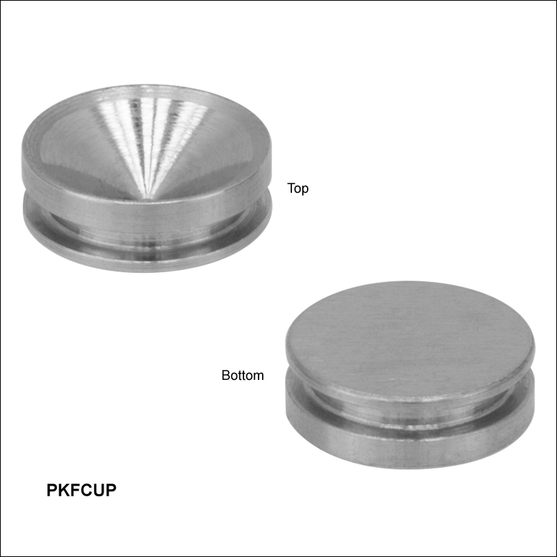
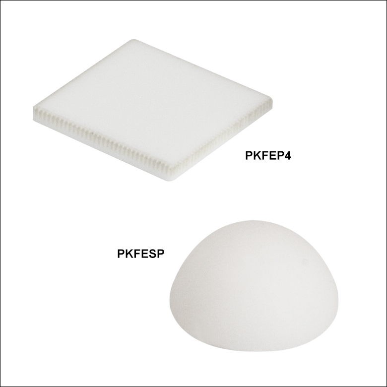
To accommodate a variety of loading conditions, additional flat ceramic or hemispherical ceramic endplates may be purchased as accessories for these chips. In addition, Thorlabs offers conical end cups, which are compatible with ball contacts possessing diameters of 3.0 mm and 5.0 mm. Please see the Operation tab for information on interfacing piezoelectric actuators with loads, special operational considerations, and data that will allow the lifetimes of these actuators to be estimated when their operational conditions are known.
Single-crystal piezoelectric chips with custom dimensions are available. Vacuum-compatible chips and stacks can also be custom ordered. Please contact Tech Support for more information. To browse our catalog offering of piezoelectric devices, see Table 1.1.
Operation Notes
Power Connections
A positive bias should be applied across the device. The positive electrode, marked by a black dot on the piezoelectric chips, should receive positive bias, and the other electrode should be connected to ground. Applying a negative bias across the device may cause mechanical failure. The single-crystal piezo stacks are shipped with wires attached: the positive electrode connected to the red wire, should receive positive bias, and the negative electrode connected to the black wire should be connected to ground.
Preloading
The maximum displacement of these actuators is achieved when they are preloaded with the maximum displacement load, which is specified for each product. The actual value of the maximum displacement varies for each item and must be experimentally determined; however, the maximum displacement will always be larger than the free stroke displacement. Preloading increases the length of the actuator's stroke because the poling process performed during fabrication does not align all ferroelectric domains in the piezoelectric crystal in the same direction. Preloading the actuator mechanically forces many of the domains into alignment. Applying a driving voltage across the piezo material causes the orientations of the ferroelectric domains to rotate so they become aligned with the applied field, and this results in a dimensional change of the piezo material. When more ferroelectric domains are initially aligned in the same direction, the dimensional change of the piezo material in response to the applied driving voltage is greater. Preloads greater than the optimal maximum displacement load result in displacements less than the maximum displacement, as higher loads oppose the switching of the grain orientations in response to the applied driving voltage.
Soldering Wire Leads to the Electrodes
If wire leads must be attached or reattached to the electrodes, a soldering temperature no higher than 370 °C (700 °F) should be used, and heat should be applied to each electrode for a maximum of 2 seconds. Solder the lead to the middle of the electrode and keep the region over which heat is applied as small as possible.
Interfacing a Piezoelectric Element with a Load
Piezoceramics are brittle and have low tensile strength. Avoid loading conditions that subject the actuator to lateral, transverse, or bending forces. When applied incorrectly, an external load that may appear to be compressive can, through bending moments, cause high tensile stresses within the piezoelectric device. Improperly mounting a load to the piezoelectric actuator can easily result in internal stresses that will damage the actuator. To avoid this, the piezoelectric actuator should be interfaced with an external load such that the induced force is directed along the actuator's axis of displacement. The load should be centered on and applied uniformly over as much of the actuator's mounting surface as possible. When interfacing the flat surface of a load with an actuator capped with a flat mounting surface, ensure the two surfaces are highly flat and smooth and that there is good parallelism between the two when they are mated. If the external load is directed at an angle to the actuator's axis of displacement, use an actuator fitted with a hemispherical end plate or a flexure joint to achieve safe loading of the piezoelectric element.
To accommodate a variety of loading conditions, flat ceramic or hemispherical ceramic end plates may be purchased as accessories for these chips. In addition, Thorlabs offers Conical End Cups which feature concave surfaces that can interface with Ø1.5 mm to Ø7.0 mm hemispherical or curved contacts. To attach a load to the piezo chip, we recommend using an epoxy that cures at a temperature lower than 80 °C (176 °F), such as our 353NDPK or TS10 epoxies or Loctite® Hysol® 9340. Loads should be mounted only to the faces of the piezoelectric chip that translate. Mounting a load to a non-translating face may lead to the mechanical failure of the actuator. Some correct and incorrect approaches to interfacing loads with piezoelectric actuators capped with both kinds of end plates are discussed in the following.

Click to Enlarge
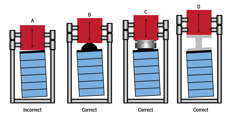
Figure 2.1 Actuation of a lever arm using a piezo element fitted with a flat plate (A, Incorrect), and a hemispherical plate (B, Correct).
Click to Enlarge
Figure 2.2 Loads properly and improperly mounted to piezo actuators using a variety of interfacing methods.
Figure 2.1 presents incorrect (A) and correct (B) methods for using a piezoelectric element to actuate a lever arm. The correct method uses a hemispherical end plate so that, regardless of the angle of the lever arm, the force exerted is always directed along the translational axis of the actuator. The incorrect interfacing of the element and the lever arm (A) endangers the piezo element by applying the full force of the load to one edge of the element. This uneven loading causes dangerous stresses in the actuator, including a bending moment around the base.
Figure 2.2 shows one incorrect (A) and three correct approaches for interfacing a flat-bottomed, off-axis load with a piezoelectric actuator. Approaches A and B are similar to the incorrect and correct approaches, respectively, shown in Figure 2.1. Correct approach C shows a conical end cup, such as the PKFCUP, acting as an interface. The flat surface is affixed to the mating surface of the load, and the concave surface fits over the hemispherical dome of the end plate. In the case of correct approach D, a flexure mount acts as an interface between the off-axis flat mounting surface of the load and the flat mounting plate of the actuator. The flexure mount ensures that the load is both uniformly distributed over the surface plate of the actuator and that the loading force is directed along the translational axis of the actuator.
Operating Under High-Frequency Dynamic Conditions
It may be necessary to implement an external temperature-control system to cool the device when it is operated at high frequencies. The maximum operating temperature of these devices is 80 °C (176 °F), and high-frequency operation causes the internal temperature of the piezoelectric device to rise. The dependence of the device temperature on the drive voltage frequency for each product can be accessed by clicking the Info icons, ![]() , below. The temperature of the device should not be allowed to exceed its specified maximum operating temperature.
, below. The temperature of the device should not be allowed to exceed its specified maximum operating temperature.
Estimating the Resonant Frequency for a Given Applied Load
A parameter of significance to many applications is the rate at which the piezoelectric actuator changes its length. This dimensional rate of change depends on a number of factors, including the actuator's resonant frequency, the absolute maximum bandwidth of the driver, the maximum current the piezoelectric device can produce, the capacitance of the piezoelectric actuator, and the amplitude of the driving signal. The length of the voltage-induced extension is a function of the amplitude of the applied voltage driving the actuator and the length of the piezoelectric device. The higher the capacitance, the slower the dimensional change of the actuator.
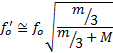
Quick changes in the applied voltage result in fast dimensional changes to the piezoelectric chip. The magnitude of the applied voltage determines the nominal extension of the chip. Assuming the driving voltage signal resembles a step function, the minimum time, Tmin, required for the length of the actuator to transition between its initial and final values is approximately 1/3 the period of resonant frequency. If there is no load applied to the piezoelectric actuator, its resonant frequency is ƒo and its minimum response time is:

After reaching this nominal extension, there will follow a damped oscillation in the length of the actuator around this position. Controls can be implemented to mitigate this oscillation, but doing so may slow the response of the actuator.
Applying a load to the actuator will reduce the resonant frequency of the piezoelectric chip. Given the unloaded resonant frequency of the actuator, the mass of the chip, m, and the mass of the load, M, the loaded resonant frequency (ƒo') may be estimated:
Estimating Device Lifetime for DC Drive Voltage Conditions
The lifetime of a piezoelectric device is a function of the operating temperature, applied voltage, and relative humidity conditions. Lifetimes are reduced as a consequence of humidity-driven electrolytic reactions, which occur at the electrodes of the piezoelectric devices when a DC voltage is applied. These reactions both generate hydrogen and result in metal dendrites growing from the cathode towards the anode. The hydrogen liberated by the electrolytic reaction chemically reacts with and degrades the piezoelectric material. Dendrites that grow to electrically connect the cathode and anode result in increasing levels of leakage current. Failed piezoelectric devices are defined as those that exhibit leakage current levels above an established threshold.
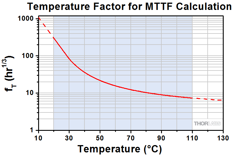
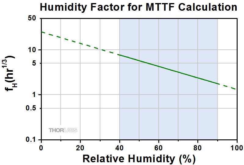
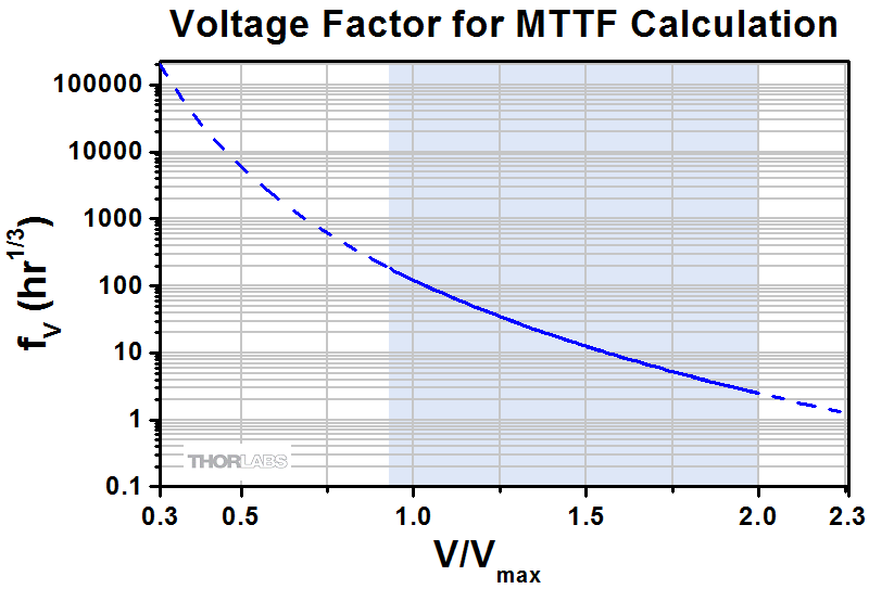
A ceramic moisture-barrier layer that insulates Thorlabs' piezoelectric devices on four sides is effective in minimizing the effects of humidity on device lifetime. As there is interest in estimating the lifetime of piezoelectric devices, Thorlabs conducted environmental testing on our ceramic-insulated, low-voltage, piezoelectric actuators. The resulting data were used to create a simple model that estimates the mean time to failure (MTTF), in hours, when the operating conditions of humidity, temperature, and applied voltage are known. The estimated MTTF is calculated by multiplying together three factors that correspond, respectively, to the operational temperature, relative humidity, and fractional voltage of the device. The fractional voltage is calculated by dividing the operational voltage by the maximum specified drive voltage for the device. The factors for each parameter can be read from the following plots, or they may be calculated by downloading the plotted data values and interpolating as appropriate.
In the following trio of plots, the solid-line segment of each curve represents the range of conditions over which Thorlabs performed testing. These are the conditions observed to be of most relevance to our customers. The dotted-line extensions to the solid-line segments represent extrapolated data and represent a wider range of conditions that may be encountered while operating the devices.
Click to Enlarge
Figure 2.3 For an Excel file containing these fT vs. temperature data, please click here.
Click to Enlarge
Figure 2.5 For an Excel file containing these fH vs. relative humidity data, please click here.
Click to Enlarge
Figure 2.4 For an Excel file containing these fV vs. V/Vmax data, please click here.
The data used to generate these temperature, voltage, and humidity factor plots resulted from the analysis of measurements obtained from testing devices under six different operational conditions. Different dedicated sets of ten devices were tested under each condition, with each condition representing a different combination of operational voltage, device temperature, and relative humidity. After devices exhibit leakage current levels above a threshold of 100 nA, they are registered as having failed. The individual contributions of temperature, humidity, and voltage to the lifetime are determined by assuming:
- MTTF = fV(V) * fT(T) * fH(H)
- A power law dependence for the voltage: fV(V) = A1Vb1
- An exponential relationship for the relative humidity: fH(T) = A2ecH
- An Arrhenius relationship for the temperature: fT(H) = A3eb2/T
where A1, A2, A3, b1, b2, and c are constants determined through analysis of the measurement data, V is the DC operational voltage, T is the device temperature, and H is the relative humidity. Because the MTTF has a different mathematical relationship with each factor, the dependence of the MTTF on each factor alone may be determined. These are the data plotted in Figures 2.3, 2.4, and 2.5. The regions of these curves marked by the blue shading are derived from experimental data. The dotted regions of the curves are extrapolated.
Lifetime testing of these devices continues, and additional data will be published here as they become available. To assist in temperature control, please see our selection of thermoelectric coolers. Temperature and humidity can be monitored using our USB Temperature and Humidity Logger.
| Posted Comments: | |
| No Comments Posted |

 Zoom
Zoom| Item # | Info | Displacement (Free Stroke)a,b |
Dimensions | Drive Voltage Range | Resonant Frequencya |
Load for Maximum Displacementc |
Blocking Forceb |
External Electrodes |
End Plates |
|---|---|---|---|---|---|---|---|---|---|
| PQ91JK | 1.2 µm ± 15% | 3.0 x 3.0 x 3.0 mm | 0 - 1000 V | 215 kHz ± 10% |
24 N (5 lbs) | 60 N (13 lbs) |
Screen-Printed Silver | None | |
| PQ91JKP3 | 1.2 µm ± 15% | 3.0d x 3.0 x 4.3 mm | 0 - 1000 V | 185 kHz ± 10% |
24 N (5 lbs) | 60 N (13 lbs) |
Copper Leads | PKJEP4 (2) |

 Zoom
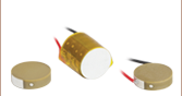
ZoomThis piezoelectric crystal stack is composed of nine piezoelectric crystals between ten copper foil electrodes. The electrodes come soldered to wire leads color-coded red for positive and black for negative. The stack has alumina end plates epoxied at either side to protect the electrodes. Due to the use of single-crystal piezo chips, the stack's motion is highly linear and nearly hysteresis free (<3% at 25 °C). Piezoelectric crystal stacks experience increased hysteresis and nonlinearity with increase in operating temperature. Hysteresis graphs taken at 25 °C and 80 °C are provided in the info icon (![]() ) below.
) below.
| Item # | Info | Displacement (Free Stroke)a,b |
Dimensions | Drive Voltage Range |
Resonant Frequencya |
Load for Maximum Displacementc |
Blocking Forceb |
External Electrodes |
End Plates |
|---|---|---|---|---|---|---|---|---|---|
| PQ9FC1 | 5.0 µm ± 15% | 5.0 x 5.0d x 7.5 mm | 0 - 500 V | 85 kHz ± 15% | 64 N (14 lbs) | 160 N (36 lbs) |
Copper Foils & Lead Wires |
PKFEP4 (2) |

 Zoom
Zoom- Compatible with Our Piezoelectric Chips and Stacks (Sold Above)
- Use with End Hemispheres Available Below
- Conical End Cups Accept Ball Contacts:
- From Ø1.5 mm to Ø3.0 mm (PKJCUP)
- From Ø2.6 mm to Ø5.0 mm (PKFCUP)
- Restricts Applied Stress to the Axial Direction
- Sold in Packs of 10
The PKJCUP and PKFCUP 416 stainless steel conical end cups are designed to be used with our piezoelectric chips and stacks when interfaced with the end hemispheres sold below. The conical cup can accept a ball contact with a diameter from 1.5 to 3.0 mm (PKJCUP) or 2.6 to 5.0 mm (PKFCUP). Using a ball contact with a piezo actuator ensures that the applied stress is restricted to the axial direction, limiting the probability of stress-induced failure. They can be affixed either to a flat face of a piezo chip or to the mechanical device that is being actuated. If affixing a cup to a chip or stack, we recommend using an epoxy that cures at a temperature lower than 80 °C (176 °F), such as 353NDPK or TS10 epoxies or Loctite® Hysol® 9340. End cups may be affixed in a similar manner to flat end plates.

 Zoom
Zoom| End Hemispheres | Flat End Plates | Compatible Components |
||
|---|---|---|---|---|
| Item # | Diameter | Item # | Dimensions | |
| PKJESP | 3.0 mm | PKJEP4 | 3.0 x 3.0 x 0.4 mm | PQ91JK PQ91JKP3a |
| PKFESP | 5.0 mm | PKFEP4 | 5.0 x 5.0 x 0.4 mm | PQ9FC1a |
- End Hemispheres and Flat End Plates
- Hemispheres Provide a Single Point of Contact for Actuation
- Flat Plates Spread Force Across Piezo Face at Contact Point
- Sold in Packs of 25
The alumina end hemispheres and flat end plates used in our piezoelectric stacks are also available separately. The hemispheres can be used to create a single contact point between a piezoelectric chip or stack and a lever arm. Alternatively, a hemisphere can be used with a compatible conical end cup (sold above). End plates are used to spread the force at the contact point over the entire surface of the piezoelectric device. When selecting an end hemisphere or flat end plate to adhere to an end face, it is important to match the bottom surface area of the hemisphere or plate to the cross section of the endface in order to ensure that forces are spread evenly over the surface. The end hemispheres have a diameter tolerance of ±0.1 mm, and the end plates have a dimensional tolerance of ±0.04 mm. To secure the end hemisphere or the flat end plate to an end face, any epoxy that cures at a temperature lower than 80 °C is considered safe to use. We suggest using Thorlabs’ 353NDPK High-Temperature Expoy or TS10 Vacuum Epoxy. Additionally, Loctite® Hysol® 9340 can also be used. Once adhered to a piezoelectric device, end plates and end hemispheres should not be removed, as it may cause damage to the device.