 Products Home / Actuators, Adjusters, & Transducers / Piezoelectric Chips and Stacks / Low-Voltage Shear Piezoelectric Chips and Stacks
Low-Voltage Shear Piezoelectric Chips and Stacks
- Shear Piezo Chips, Discrete Stacks, or Multi-Axis Positioners
- 1D-Lateral, 2D-Lateral, or 3D Displacement
- Chips Available Unwired, with or without Flat End Plates
- Stacks with Lead Wires and Flat End Plates
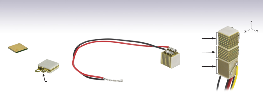
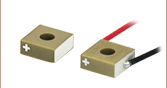
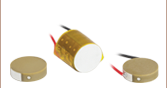
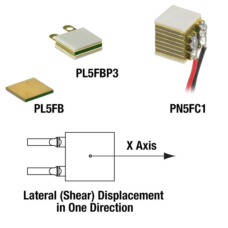
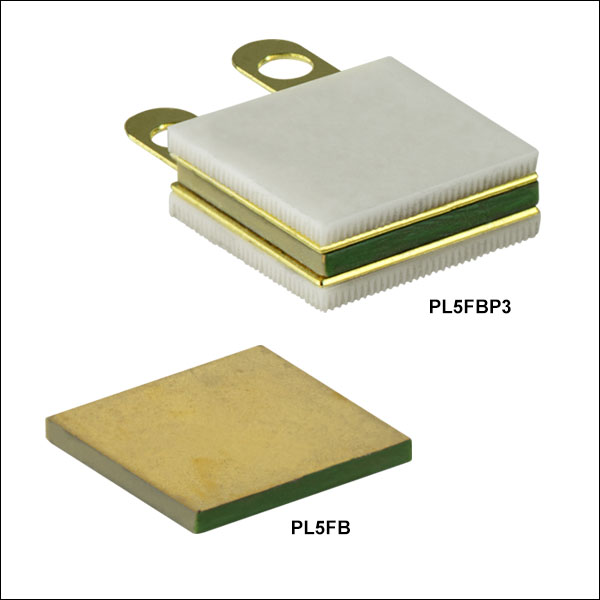
PL5FBP3
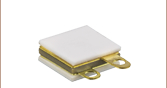
Chip with Two Flat End Plates
Copper Plates with Leads (Indicated)
for Electrical Connections
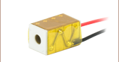
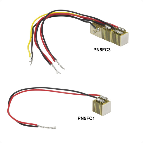
PN5FC1
Discrete Shear Stack Translates along One Lateral Direction
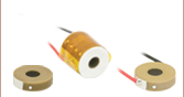
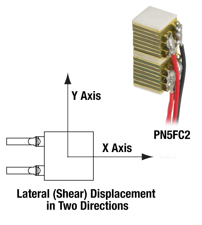
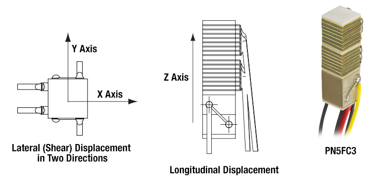
PN5FC3
One Longitudinally- and Two Laterally-Translating Stacks Bonded Together for 3D Positioning of Top Surface
X-Axis
Y-Axis
Segment Displacement is Parallel to:
Z-Axis
PL5FB
Chip with Bare Gold Top and Bottom Electrodes


Please Wait
| Piezo Selection Guide |
|---|
| Piezoelectric Ceramic Chips |
| Square |
| Square with Through Hole |
| Round |
| Ring |
| Tube |
| Shear |
| Benders |
| Single-Crystal Piezoelectric Chips |
| Square |
| Piezoelectric Ceramic Stacks |
| Discrete, Square |
| Discrete, Square with Through Hole |
| Discrete, Round |
| Discrete, Ring |
| Discrete, Hermetically Sealed |
| Discrete, Shear (1D to 3D Positioners) |
| Co-Fired: Square, Square with Through Hole, Round, & Ring |
| Co-Fired or Discrete: Square with Strain Gauges |
| Piezoelectric Crystal Stacks |
| Square |
| Mounted Piezoelectric Actuators |
| Ultrasonic Piezo Chips & Transducers |
| Vibrating Piezo Actuator |
Click to Enlarge
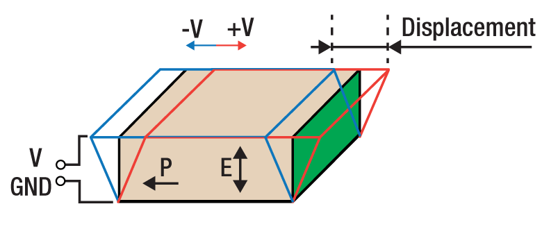
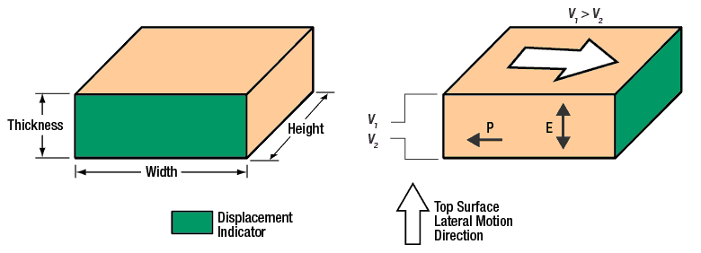
Shear Piezoelectric Chips and Stacks provide lateral displacement. The relationships between voltage bias (±V), piezo polarization (P) and electric field (E) are shown. The green side on our chips indicates displacement direction. See the Operation tab for details.

Features
- Low Drive Voltages for Piezo Chips, Stacks, and Multi-Axis Positioners
- ±200 V Range for Shear Piezo Chips and Single Stacks
- ±200 V Range for Each Shear Piezo Stack Included in Item #s PN5FC2 & PN5FC3
- 0 V to 150 V for the Longitudinally-Translating Stack Included in Item # PN5FC3
- Sub-Micron Resolution Displacement
- 5.0 mm × 5.0 mm Mounting Face
- For Use in Open-Loop Experimental Setups
- Custom Size Options Available by Contacting Tech Support
- Flat End Plate also Available Separately
Thorlabs offers Shear Piezoelectric Chips and Stacks as well as Multi-Axis Positioners that incorporate our shear piezo stacks. Our shear piezo chips provide up to 1.3 µm of displacement along one lateral axis, while our shear piezo stacks achieve a lateral stroke up to 7.0 µm. Our multi-axis positioners achieve 7.0 µm displacement per axis. For a complete list of specifications, please see the tables below.
Please see the Operation tab for information on interfacing piezoelectric actuators with loads and special operational considerations. Piezoelectric chips with custom dimensions, voltage ranges, and coatings are available; please contact Tech Support for details.
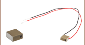
Shear Piezo Chips
The polarity of the voltage bias controls whether the shear piezo chips and stacks provide positive or negative displacement along the lateral translation axis. The diagram above illustrates the response of a piezo chip to a voltage applied across its electrodes, which are located on the top and bottom surfaces. When the bottom surface is fixed in place, positively biasing the top surface results in it translating over the side marked with the green bar. When negatively biased, the top surface moves in the opposite direction.
Shear Piezo Stacks and Multi-Axis Positioners
Our shear piezo stacks consist of multiple discrete shear piezo chips bonded together using epoxy and copper foils. Epoxy is also used to glue flat alumina end plates to the top and bottom surfaces of the stacks. As is the case for our chips, a single shear piezo stack can be forward or reverse biased to provide displacement in a positive or negative direction along a single lateral axis. Positioners providing displacement along both lateral axes mate the upper end plate of one shear piezo stack to the lower end plate of another. Thorlabs' three-axis positioner bonds two shear and one longitudinally-translating discrete piezo stacks together, with the last providing translation in the direction normal to the surfaces of the stacks. Please note that the longitudinally-translating stack provides displacement only along the positive displacement axis. This stack cannot be reverse biased, and it has a different drive voltage range than the shear piezo stacks. Two wire leads are attached to each stack, which allows the stacks to be individually controlled for fine positioning of the top surface of the positioner.
Shear vs. Axial Strain
In shear piezo elements, there is an orthogonal relationship between the polarization direction of the piezo material and the direction of the electric field induced by the voltage bias. When shear piezos are operated as specified, applying a voltage bias across the electrodes creates a shear strain in the piezo element. This happens as microscopic, and reversible, changes in the piezo material occur to better align its overall polarization direction with the direction of the applied electric field. In contrast, the more common longitudinally-translating piezo chips are operated by applying an electric field parallel to the polarization direction of the piezo material, which results in displacement along that same axial direction normal to the surface of the electrodes. Please note that hysteresis from the shear strain of piezo ceramics can be up to 40%. This is greater than the hysteresis that results from the axial strain of piezos, which provides longitudinal displacement.
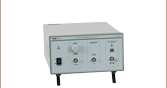
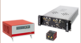
Piezo Drivers
We generally recommend Thorlabs' HVA200 High-Voltage Amplifier to drive the shear piezo chips and stacks. For the PN5FC3 multi-axis piezo positioner, note that while the HVA200 can drive the stack in the longitudinal direction, the relatively low current provided by the HVA200 combined with the high capacitance of the stack limits the maximum driving voltage frequency. In addition, care must be taken not to exceed the driving voltage limits of this stack. Drivers better compatible with the longitudinally-translating stack incorporated in the PN5FC3 include the MDT69xB or KPZ101 Open-Loop Controllers, and the BPC301 and BPC303 Closed-Loop Controllers are also options.
| X-Axis Positioning | X- and Y-Axis Positioning | X-, Y-, and Z-Axis Positioning |
|---|---|---|
 Click to Enlarge |
 Click to Enlarge |
 Click to Enlarge |
Shear Chips and the PN5FC1 single shear stack offer displacement along one lateral direction, the PN5FC2 comprises two bonded shear stacks and provides displacement along both lateral directions, and the PN5FC3 enables 3D positioning by bonding a longitudinally-translating stack to two laterally-translating shear stacks.
Click to Enlarge
Figure 1: A green bar indicates the lateral motion direction of the shear piezos. The surface electrode that has a positive voltage applied to it will be laterally displaced towards the painted green bar.
Operation Notes
Electrical Bias and Shear Strain
Thorlabs' shear piezo chips have chemically deposited gold electrodes on the top and bottom 5 mm x 5 mm surfaces. When a voltage (±200 V maximum) is applied across these electrodes, a shear strain is created in the piezo material. The deformation induced by the shear strain causes two parallel side surfaces to tilt in unison, which causes the top surface to translate laterally with respect to the bottom surface.
This lateral motion, which is characteristic of shear piezos, is a consequence of the applied electric field (E) being perpendicular the polarization (P) of the piezo material. The relationships among the polarization direction, the applied electric field, and the direction of the lateral displacement of the chip’s surface is shown in Figure 1. When the electric field is applied so that the electrode on the top surface is positively biased, the top surface will translate over the side of the chip marked by the green bar; the top surface will move laterally in the direction indicated by the white arrow. Please note that using one 5 mm x 5 mm surface of the chip to translate a load requires the opposite surface to be mounted to a fixed surface. See the Interfacing a Piezoelectric Element with a Load or Mating Surface section below for more details.
These shear piezo chips have identical electrodes on their top and bottom surfaces, and the induced shear strain is symmetrical. Therefore, these chips can be driven by bipolar symmetrical electrical supplies. We recommend Thorlabs' HVA200 High-Voltage Amplifier, which is available below.
Click to Enlarge
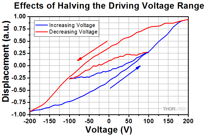
Figure 2 Example plot illustrating that the stroke for a ±100 V driving voltage range is approximately 30% that for a ±200 V range. Relative hysteresis under both operating conditions is also shown.
Hysteresis and Lateral Displacement
The displacement of a piezo chip or stack depends on both the instantaneous driving voltage and how the element was driven in the past. This hysteresis is a consequence of the intrinsic properties of the piezo element. The Displacement vs. Voltage graphs, provided in the tables below, give the hysteresis exhibited by the lateral displacement of the top surface of a shear piezo chip or stack when the bottom surface is fixed and the driving voltage is varied from -200 V to 200 V. Hysteresis from the shear strain of piezo ceramics can be up to 40%, which is greater than that from the axial strain of piezos. This must be considered when driving shear piezo devices.
As is illustrated by the graph on the left, reducing the driving voltage range from ±200 V to ±100 V decreases the total displacement to approximately 30% of the maximum rated stroke.
Adding an Electrical Connection to the PL5FB External Electrodes
The PL5FB does not have a flat plate on the mounting surfaces and therefore does not have copper leads. Electrical connection to the external electrodes on the PL5FB can be achieved by using mechanical contacts, gluing with electrically conductive glues, or wire bonding. Directly soldering on the contact surface will affect the flatness and load distribution, thus negatively impacting performance.
Soldering Wire Leads to the PL5FBP3 Electrodes
The PL5FBP3 has a flat mounting plate on the mounting surfaces and therefore includes copper leads on the electrodes for electrical connections. If wire leads must be attached to the electrodes, a soldering temperature no higher than 370 °C (700 °F) should be used, and heat should be applied to each electrode for a maximum of 2 seconds. Solder the lead to the middle of the electrode and keep the region over which heat is applied as small as possible.
Caution: After driving, the piezo is fully charged. Directly connecting the positive and negative wire leads has the risk of electricity discharging, spark, and even failure. We recommend using a resistor (>1 kΩ) between the wires to release the charge.
Interfacing a Piezoelectric Element with a Load
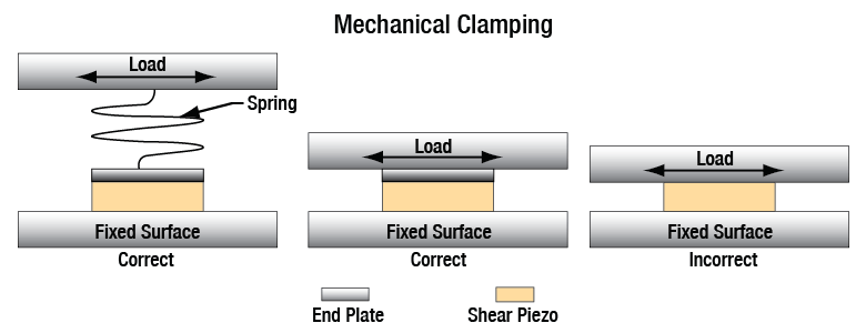
As the top and bottom surfaces of shear piezo chips move relative to one another, one surface must be mounted to a fixed substrate to use the chip as an actuator. The shear piezo chips can be mounted either by mechanical clamping or gluing. Correct and incorrect examples are shown and described below.
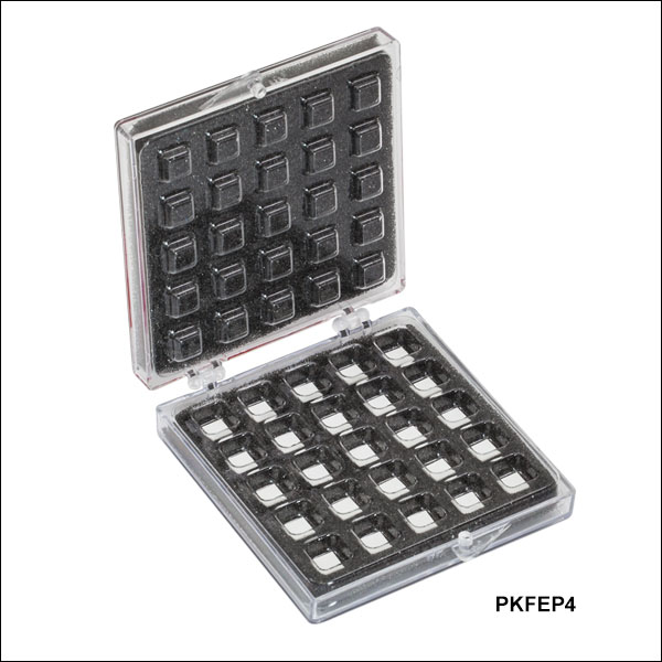
The load should be centered on and applied uniformly over as much of the chip’s mounting surface as possible. The direction of the loading should be normal to the loading surface of the chip. The mating surfaces of both the actuator and the load or surface must be highly flat and smooth with surface roughness less than 10 µm and a Mohs hardness higher than 6. We recommend using alumina endplates (item # PKFEP4), which have a Mohs hardness of 9 and will cap the contact surfaces with an insulating layer. Alternately, insulation can also be achieved using a polyimide film. Ensure good parallelism between the two mating surfaces before applying pressure.
When taking a mechanical clamping approach, the axial stress induced by the clamp must be well controlled. Too little pressure can lead to slippage, whereas too much pressure can damage the ceramic. With the appropriate contact surface, and in the case of low shear force, a pressure of 1 to 3 MPa is recommended. The stiffness of the loading mechanism in the actuation direction should be as low as possible in order not to hinder the movement of the piezo actuator.
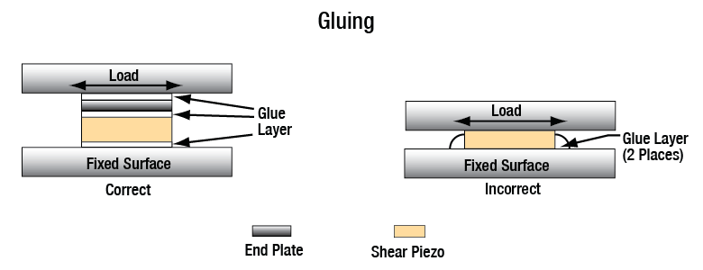
When gluing the piezo in place it is important to apply a very thin glue layer between the shear chip and the substrate, as shown below. This is generally ensured by using low viscosity glue. Some pressure (e.g. less than 3 MPa) should be applied during the curing process. To attach a load to the piezo chip, we recommend using an epoxy that cures at a temperature lower than 80 °C (176 °F), such as our 353NDPK, TS10, or G14250 epoxies or Loctite® Hysol® 9340. Loads should be mounted only to the faces of the piezoelectric chip that translate. Mounting a load to a non-translating face may lead to the mechanical failure of the actuator.
Some correct and incorrect approaches to interfacing loads with piezoelectric chips are shown in the diagrams below.
Click to Enlarge
Figure 3 Correct mechanical clamping methods include using a spring to apply force. Note that the incorrect example on the right is missing an end plate between the chip and load.
Click to Enlarge
Figure 4 The piezo should be held in place using adhesives as shown on the left. Note that applying glue as shown on the right will impede the lateral translation of the piezo.
Cleaning for Vacuum Compatibility
When suitable for vacuum applications, Thorlabs' piezo chips have the rated vacuum compatibility specified in their Info Icons (![]() ). While no extra cleaning is needed to achieve this value, we recommend cleaning these products with isopropyl alcohol (IPA) in an ultrasonic immersion tank and then baking it at 60 °C for two hours. Do not immerse the device in other organic solvents.
). While no extra cleaning is needed to achieve this value, we recommend cleaning these products with isopropyl alcohol (IPA) in an ultrasonic immersion tank and then baking it at 60 °C for two hours. Do not immerse the device in other organic solvents.
| Posted Comments: | |
Julien Camard
(posted 2023-01-17 15:30:33.83) Hi, I would like some guidance on connecting a resistor (>1 kΩ), as advised, to the 3 axis piezo stack. I unfortunately damaged the longitudinal stack and had to order a new one. Although this was due to a voltage spike on the generator side, can you please advise if any other strategy can be set up to avoid damage to the piezo? Thanks. cdolbashian
(posted 2023-01-23 01:22:22.0) Thank you for your inquiry. we will reach out to you directly to trouble shoot your issue. user
(posted 2022-06-27 10:48:36.607) Hi, We used a stack of two PL5FB chips in ultra-high vacuum, and baked them at 120C (which is below the working temperature) for a couple of weeks. Unfortunately, the chips did not survive the bakeout; the travel range is reduced to less than 1nm. What temperature and duration do you recommend for vacuum bakeout of these shear piezos? Thank you! cdolbashian
(posted 2022-07-06 11:21:10.0) Thank you for contacting Thorlabs. Sorry to hear about the issue. 120℃ should be fine. In general, we recommend cleaning the part with isopropyl alcohol (IPA) in an ultrasonic immersion tank and then bake it at 60 °C for two hours. We will reach out to you directly to help diagnose the issue further. user
(posted 2022-02-22 05:42:46.503) Hi. These chips and staks have resonant frequency of up to ~2MHz, but the driver you suggest (HVA200) has 1MHz bandwidth. How can I drive these chips/stacks with 2MHz frequency? Thank you cdolbashian
(posted 2022-02-24 04:58:24.0) Thank you for your inquiry. For these chips and stacks, they cannot be operated at the resonant frequency, as this generates a lot of heat and causes the device to fail. We recommend operating frequency less than 1/3 of the resonant frequency: HVA200 is usually sufficient. For the Z axis of PN5FC3, please note that the HVA200 combined with the high capacitance of the stack limits the maximum driving voltage frequency. Under such high frequency, the displacement would need to be reduced as the response time of the piezo will be longer than the period. I see that you didn't leave your contact information for us to reach you. Please feel free to get in touch with your local tech support team (in your case, techsupport.uk@thorlabs.com) if you would like a shear piezo that works under 2MHz, we could assess if it’s possible to do such customization. benalunda10
(posted 2017-12-03 04:37:48.693) Hi,
Thank you so much for your earlier response. I however have one more question. Could you kindly let me know the shear modulus of Al2O3, PL5FB and the copper alloy used for the electrodes. Thank you. nbayconich
(posted 2017-12-08 08:02:04.0) Thank you for contacting Thorlabs. The shear modulus for AL2O3 is 124GPa and for Copper is 45GPa-48Gpa. benlaunda10
(posted 2017-06-07 13:02:00.153) Hello,
The information here is very useful. However, I have a question about PL5FBP3. What are the material properties for the end flat plates? I would like to know about the Young's modulus and Poisson's ratio and any other useful property regarding mechanical properties.
I would also like know about the piezo-coefficient for the PL5FB shear piezos.
Thank you.
Ben nbayconich
(posted 2017-06-27 08:06:55.0) Thank you for contacting Thorlabs. PL5FBP3 use Al2O3 as end plate, with Young's modulus of 375GPa, Poisson's ratio of 0.2. The piezo-coefficient for PL5FB is D33~710pC/N, d31~-320pC/N, d15~900pC/N. A Techsupport representative will contact you directly. |

 Zoom
Zoom| Webpage Features | |
|---|---|
| Clicking this icon below will open a window that contains item specific specifications and mechanical drawings. | |
- Provides Lateral Displacement in the Plane of the Top Surface
- Bias Voltage Polarity Controls Direction of Stroke
- Positively Biased Surface Translates Towards the Green Bar
- Negatively Biased Surface Translates in Direction Opposite the Green Bar
- Suitable for Vacuum Applications
- Available with or without Flat End Plates and Copper Foils with Leads
Each piezo chip is fabricated from a single layer of piezoelectric ceramic with chemically deposited gold electrodes on the top and bottom of the chip. The driving voltage is applied across these electrodes. The PL5FBP3 includes flat end plates (Item # PKFEP4) with copper plates and leads glued to the top and bottom of the piezo. The end plates spread the contact force of the load over the entire mounting face of the piezo while the copper leads, which are extended beyond the footprint of the chip, facilitate making electrical connections.
Applying a voltage less than -200 V or greater than 200 V to either electrode will decrease the the life of these chips and may cause mechanical failure.
| Item #a,b | Info | End Plates | Shear Displacement (Free Stroke)c |
Dimensions | Drive Voltage Range |
Resonance Frequency | Max Shear Loade | Max Axial Loadf |
|---|---|---|---|---|---|---|---|---|
| PL5FB | No | 1.3 µm ± 20% | 5.0 mm x 5.0 mm x 0.5 mm | ±200 V | 1800 kHz | 50 N (11.3 lbs) | 1000 N (225 lbs) | |
| PL5FBP3 | Two PKFEP4 | 5.0 mm x 8.0 mmd x 1.8 mm | 1900 kHz |
- For complete specifications, please see the Info Icons (
 ) above.
 - We recommend using the HVA200 High-Voltage Amplifier (available below) with these piezos. Please note that the actuators sold on this page do not contain a strain gauge and therefore will not provide positional feedback.
- The "free stroke" displacement corresponds to conditions of no load and while operating over the full specified driving voltage range.
- This dimension includes the length of the copper leads.
- Max Allowed Load Applied in the Lateral Direction, Resisting Lateral Displacement
- Max Allowed Load Applied in the Direction Normal to the Plane of the Flat End Plates, Towards the Piezo Element, During Lateral Displacement

 Zoom
Zoom| Webpage Features | |
|---|---|
| Clicking this icon below will open a window that contains item specific specifications and mechanical drawings. | |
- Position the Top Surface in One, Two, or Three Dimensions
- PN5FC1 Provides Lateral Stroke along X Axis and Includes One Shear Piezo Stack
- PN5FC2 Provides Lateral Stroke along X and Y Axes and Includes Two Shear Piezo Stacks
- PN5FC3 Provides 3D Positioning and Includes One Longitudinal and Two Shear Piezo Stacks
- Control Shear Stack's Stroke Direction along Lateral Translation Axis via Voltage Bias Polarity
- Longitudinally-Translating Stack of the PN5FC3 Must Only be Forward Biased
- Lead Wires Attached to Each Stack Allow Independent Control of Each Stack in the Positioner
- Two Flat Alumina End Plates Facilitate Mounting
Our multi-axis positioners provide displacement along the axes of an orthogonal coordinate system, with each integrated stack providing displacement along a single axis. The translation axes of the individual stacks and the stacks built into our multi-axis positioners can be identified from the wire configuration.
All positioners include one or two shear stacks. Applying a voltage less than -200 V or greater than 200 V to either electrode of a shear stack will decrease its lifetime and may cause mechanical failure. Our PN5FC3 also includes a longitudinally-translating stack, which provides displacement in the Z-axis direction. Applying a voltage greater than 150 V to this longitudinally-translating stack will decrease the life of the stack and may cause mechanical failure, and, unlike the shear stacks, applying a reverse bias may cause this stack to mechanically fail.
Cross talk between the two shear stacks bonded together in the PN5FC2 and PN5FC3 is no more than 5%.
| Item #a,b | Info | Displacement (Free Stroke)c |
Dimensionsd | Drive Voltage Range |
Resonance Frequency |
Max Loads for Lateral Displacement |
Recommended Load for Longitudinal Displacementg |
Blocking Force for Longitudinal Displacementh |
|
|---|---|---|---|---|---|---|---|---|---|
| Sheare | Axialf | ||||||||
| PN5FC1 | X Axis: 7.0 µm ± 20% | X-Axis Width: 7.3 mm (Max) Y-Axis Width: 5.4 mm (Max) Length: 6.0 mm ± 0.1 mm |
X Axis: ±200 V | X Axis: 2100 kHz | 50 N (11.3 lbs) |
1000 N (225 lbs) |
N/A | N/A | |
| PN5FC2 | X Axis: 7.0 µm ± 20% Y Axis: 7.0 µm ± 20% |
X-Axis Width: 7.3 mm (Max) Y-Axis Width: 5.4 mm (Max) Length: 12.0 mm ± 0.1 mm |
X Axis: ±200 V Y Axis: ±200 V |
X Axis: 2100 kHz Y Axis: 2100 kHz |
|||||
| PN5FC3 | X Axis: 7.0 µm ± 20% Y Axis: 7.0 µm ± 20% Z Axis: 7.0 µm ± 20% |
X-Axis Width: 7.3 mm (Max) Y-Axis Width: 8.5 mm (Max) Length: 18.0 mm ± 0.1 mm |
X Axis: ±200 V Y Axis: ±200 V Z Axis: 0 V to 150 V |
X Axis: 2100 kHz Y Axis: 2100 kHz Z Axis: 125 kHz |
400 N (90 lbs) |
1000 N (225 lbs) |
|||
- For complete specifications, please see the Info Icons () above.
- We recommend using the HVA200 High-Voltage Amplifier (available below) with these piezos. Please note that the actuators sold on this page do not contain a strain gauge and therefore will not provide positional feedback.
- The "free stroke" displacement corresponds to conditions of no load and while operating over the full specified driving voltage range.
- These dimensions include the maximum thicknesses of the outer coating and wire attachment points.
- Max Allowed Load Applied in the Lateral Direction, Resisting Lateral Displacement
- Max Allowed Load Applied in the Direction Normal to the Plane of the Flat End Plates, towards the Piezo Element
- Displacement may vary slightly for different loads. Recommended load gives maximum Z-axis displacement.
- At Max Voltage

 Zoom
Zoom| Item # | Dimensions | Compatible Piezo Chips |
|---|---|---|
| PKFEP4 | 5.0 mm x 5.0 mm x 0.4 mm | TA0505D024(W), PA4FE(W), PA4FK(W), PL5FB |
- 5 mm x 5 mm x 0.4 mm Flat End Plate
- Flat Plates Spread Force Across Piezo Face at Contact Point
- Mohs Hardness of 9
This Alumina Flat End Plate is designed to spread the force at the contact point over the entire surface of the piezo chip. It is used on the top and bottom surface of the PL5FBP3 piezo chip above and has a dimensional tolerance of ±0.04 mm.