 Products Home
Mid-IR Photovoltaic Detectors, HgCdTe (MCT)
- HgCdTe (MCT) Detectors with Optically Immersed Sensors
- Models Available with Four-Stage TEC
- Available in TO-8 or TO-39 Package
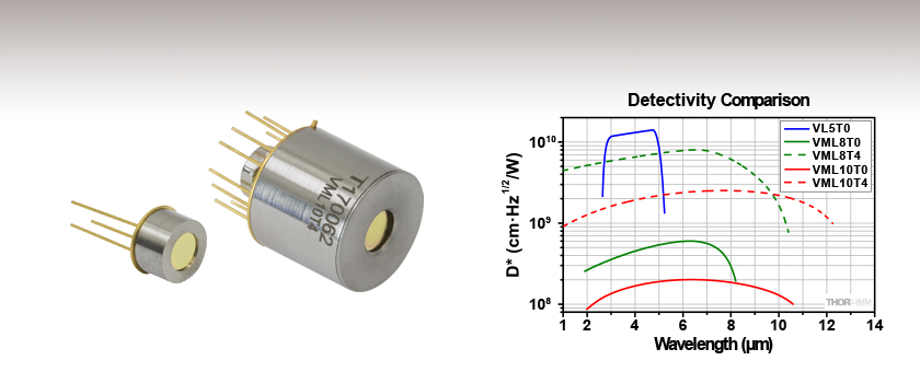
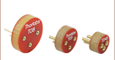
VL5T0
2.7 - 5.0 µm Wavelength Range,
TO-39 Package
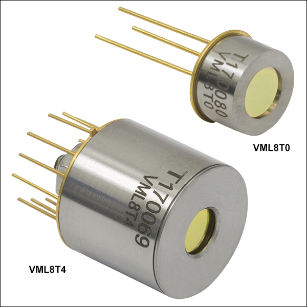
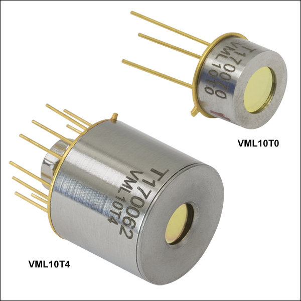
VML10T4
2.0 - 10.6 µm Wavelength Range
with Thermoelectric Cooling,
TO-8 Package


Please Wait
| Mounted and Unmounted Detectors |
|---|
| Unmounted Photodiodes (200 - 2600 nm) |
| Calibrated Photodiodes (350 - 1800 nm) |
| Mounted Photodiodes (200 - 1800 nm) |
| Thermopile Detectors (0.2 - 15 µm) |
| Photovoltaic Detectors (2.0 - 10.6 µm) |
| Pigtailed Photodiodes (320 - 1000 nm) |
Click for Details
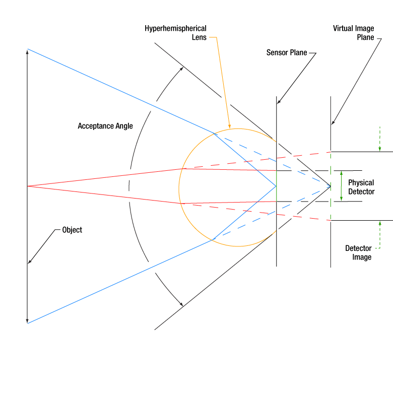
A hyperhemispherical lens forms an image on a virtual plane behind the sensor element, resulting in an effective optical area greater than the physical sensor area.
Click for Details
A standard hemispherical immersion lens forms an image in the plane of the sensor element.
Features
- Photovoltaic Detectors Optimized for Mid-IR Wavelength Ranges
- Integrated GaAs Microlens Improves Detectivity by an Order of Magnitude
- Increased Detectivity on Models with Four-Stage Thermoelectric Cooling (TEC)
- Mounted in a Hermetically Sealed Package with a Wedged ZnSe Window
These photodiodes operate in photovoltaic mode and provide coverage for Mid-IR wavelengths through 10.6 µm. The detectors are optimized for best performance at a specific wavelength (5.0 µm, 8.0 µm, or 10.6 µm). Each HgCdTe (MCT) sensor element is integrated with a hyperhemispherical GaAs lens to achieve optical immersion, and each detector is provided with a wedged ZnSe window that is AR-coated for the 2 - 13 µm wavelength range. Our 8.0 µm and 10.6 µm detectors are also available with integrated four-stage thermoelectric coolers (TECs) to maintain the detector elements at -78 °C, as cooling improves detector current responsivity and therefore detectivity. Our MCT detectors with and without TEC are offered in TO-8 or TO-39 packages, respectively. We also incorporate the VML8T0 and VML10T0 detectors in our PDAVJ Series Amplified Photodetectors.
Each detector includes a printed test report including measured responsivity and detectivity plots, as well as other electrical characteristics. Click here for a sample test report.
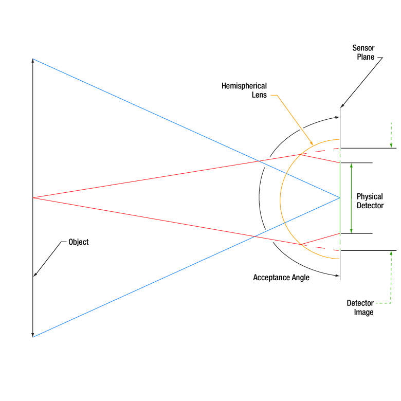
Optically Immersed Sensor Element
Optical Immersion is used in these MCT detectors to produce a 1 mm2 effective detector area, approximately two orders of magnitude larger than the actual sensor, resulting in increased responsivity. This technique is performed by integrating the sensor element with a GaAs hyperhemispherical microlens, which has a high refractive index (n = 3.3) and is transparent to Mid-IR wavelengths. The diagrams to the right illustrate the benefit of using a hyperhemispherical lens, rather than a hemispherical lens. A hemispherical lens focuses light onto the sensor plane (left diagram) and produces an image with dimensions larger than the physical sensor by a factor of n. The hyperhemispherical lens (right diagram) forms an image on a virtual focal plane located behind the sensor, and this image has dimensions larger than the physical sensor by a factor of n2. Note that the acceptance angle is reduced to 35° by the hyperhemispherical lens, in contrast to the 180° acceptance angle that would be obtained if a hemispherical lens were used.
Detectors with TECs
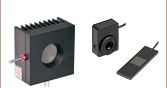
The VML8T4 and VML10T4 detectors feature integrated four-stage TECs, which enable their operating temperatures of -78 °C. Cooling to this temperature results in an order of magnitude increase in detectivity as a result of improved current responsivity. For more details, refer to the TE Cooling tab and Pin Diagrams tabs above. We recommend using our TED4015 Temperature Controller to regulate the detector temperature.
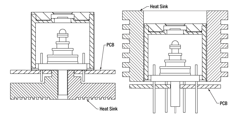
Incorrect Heat Sink Placement
Click for Details
The heat sink should not predominantly contact the mounting screw or the cylindrical housing.
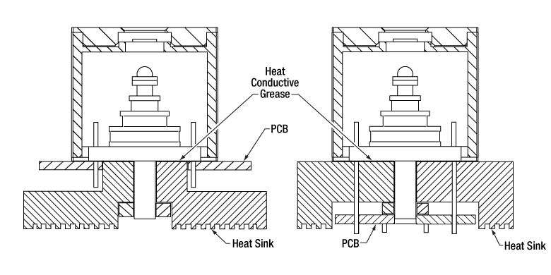
Correct Heat Sink Placement
Click for Details
The heat sink must adequately contact the base of the detector package using thermal grease or heat conductive epoxy.
Heat Sink Placement
The four-stage thermoelectric (TEC) cooler integrated into the VML8T4 and VML10T4 detectors transfers heat from the sensor chip to the underside of the detector package. To help dissipate this heat, a heat sink should be firmly in contact with a large portion of the bottom, as illustrated in the first two diagrams to the right. Thermal grease or heat conductive epoxy should be used between the detector housing and the heat sink to maximize heat transfer.
Click for Details
Click Here for Raw Data
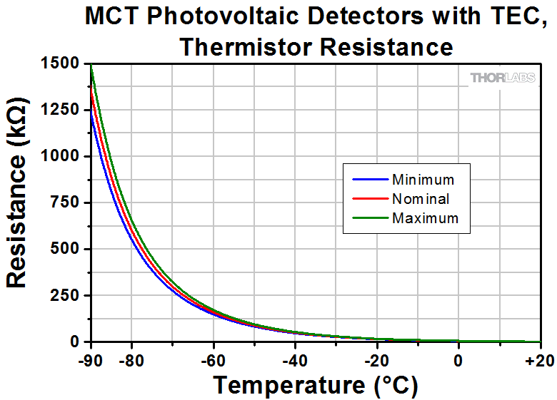
This graph specifies resistance vs. temperature for the Murata NCP03XM222E05RL thermistor incorporated in our VMLxT4 detectors. The raw data file above also includes resistance values calculated using the β-parameter equation.
Temperature Control
The TEC maintains the operating temperature by operating in closed loop mode, in which the integrated NTC thermistor (Murata, NCP03XM222E05RL) provides temperature feedback. We recommend using our TED4015 Temperature Controller to maintain a detector temperature of -78 °C. The temperature probe type should be set to NTC thermistor, with calibration values T0 = 25 °C, R0 = 2.2 kΩ, and β = 3080 K (approximate value at 25/-78 °C). These values can be used to correlate the thermistor's resistance with the MCT diode temperature using the β-parameter equation below, or the graph and raw data below and to the right.

MCT Photovoltaic Detector Pin Diagrams
Both views shown below are looking at the connector from the bottom side.
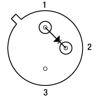
VL5T0, VML8T0, and VML10T0 Detectors (TO-39 Package)
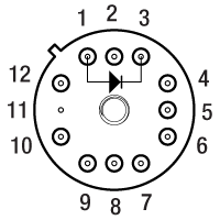
VML8T4 and VML10T4 Detectors with Integrated TEC (TO-8 Package)
| TO-39 Detector Pins | |
|---|---|
| Pin | Connection |
| 1 | Detector Anode |
| 2 | Detector Cathode |
| 3 | Ground/Case |
| TO-8 Detector Pins | |||
|---|---|---|---|
| Pin | Connection | Pin | Connection |
| 1 | Detector Anode | 7 | Thermistor Pin 1 |
| 2 | TE Cooler (+) | 8 | TE Cooler (-) |
| 3 | Detector Cathode | 9 | Thermistor Pin 2 |
| 4 | Not Used | 10 | Not Used |
| 5 | Not Used | 11 | Ground |
| 6 | Not Used | 12 | Not Used |
Photodiode Tutorial
Theory of Operation
A junction photodiode is an intrinsic device that behaves similarly to an ordinary signal diode, but it generates a photocurrent when light is absorbed in the depleted region of the junction semiconductor. A photodiode is a fast, highly linear device that exhibits high quantum efficiency and may be used in a variety of different applications.
It is necessary to be able to correctly determine the level of the output current to expect and the responsivity based upon the incident light. Depicted in Figure 1 is a junction photodiode model with basic discrete components to help visualize the main characteristics and gain a better understanding of the operation of Thorlabs' photodiodes.
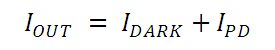
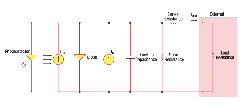
Figure 1: Photodiode Model
Photodiode Terminology
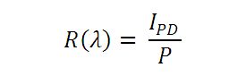
Responsivity
The responsivity of a photodiode can be defined as a ratio of generated photocurrent (IPD) to the incident light power (P) at a given wavelength:
Modes of Operation (Photoconductive vs. Photovoltaic)
A photodiode can be operated in one of two modes: photoconductive (reverse bias) or photovoltaic (zero-bias). Mode selection depends upon the application's speed requirements and the amount of tolerable dark current (leakage current).
Photoconductive
In photoconductive mode, an external reverse bias is applied, which is the basis for our DET series detectors. The current measured through the circuit indicates illumination of the device; the measured output current is linearly proportional to the input optical power. Applying a reverse bias increases the width of the depletion junction producing an increased responsivity with a decrease in junction capacitance and produces a very linear response. Operating under these conditions does tend to produce a larger dark current, but this can be limited based upon the photodiode material. (Note: Our DET detectors are reverse biased and cannot be operated under a forward bias.)
Photovoltaic
In photovoltaic mode the photodiode is zero biased. The flow of current out of the device is restricted and a voltage builds up. This mode of operation exploits the photovoltaic effect, which is the basis for solar cells. The amount of dark current is kept at a minimum when operating in photovoltaic mode.
Dark Current
Dark current is leakage current that flows when a bias voltage is applied to a photodiode. When operating in a photoconductive mode, there tends to be a higher dark current that varies directly with temperature. Dark current approximately doubles for every 10 °C increase in temperature, and shunt resistance tends to double for every 6 °C rise. Of course, applying a higher bias will decrease the junction capacitance but will increase the amount of dark current present.
The dark current present is also affected by the photodiode material and the size of the active area. Silicon devices generally produce low dark current compared to germanium devices which have high dark currents. The table below lists several photodiode materials and their relative dark currents, speeds, sensitivity, and costs.
| Material | Dark Current | Speed | Spectral Range | Cost |
|---|---|---|---|---|
| Silicon (Si) | Low | High Speed | Visible to NIR | Low |
| Germanium (Ge) | High | Low Speed | NIR | Low |
| Gallium Phosphide (GaP) | Low | High Speed | UV to Visible | Moderate |
| Indium Gallium Arsenide (InGaAs) | Low | High Speed | NIR | Moderate |
| Indium Arsenide Antimonide (InAsSb) | High | Low Speed | NIR to MIR | High |
| Extended Range Indium Gallium Arsenide (InGaAs) | High | High Speed | NIR | High |
| Mercury Cadmium Telluride (MCT, HgCdTe) | High | Low Speed | NIR to MIR | High |
Junction Capacitance
Junction capacitance (Cj) is an important property of a photodiode as this can have a profound impact on the photodiode's bandwidth and response. It should be noted that larger diode areas encompass a greater junction volume with increased charge capacity. In a reverse bias application, the depletion width of the junction is increased, thus effectively reducing the junction capacitance and increasing the response speed.
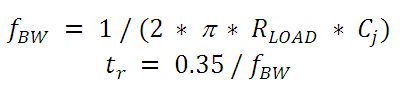
Bandwidth and Response
A load resistor will react with the photodetector junction capacitance to limit the bandwidth. For best frequency response, a 50 Ω terminator should be used in conjunction with a 50 Ω coaxial cable. The bandwidth (fBW) and the rise time response (tr) can be approximated using the junction capacitance (Cj) and the load resistance (RLOAD):
Noise Equivalent Power
The noise equivalent power (NEP) is the generated RMS signal voltage generated when the signal to noise ratio is equal to one. This is useful, as the NEP determines the ability of the detector to detect low level light. In general, the NEP increases with the active area of the detector and is given by the following equation:

Here, S/N is the Signal to Noise Ratio, Δf is the Noise Bandwidth, and Incident Energy has units of W/cm2. For more information on NEP, please see Thorlabs' Noise Equivalent Power White Paper.
Terminating Resistance
A load resistance is used to convert the generated photocurrent into a voltage (VOUT) for viewing on an oscilloscope:
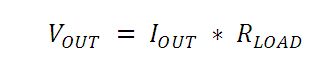
Depending on the type of the photodiode, load resistance can affect the response speed. For maximum bandwidth, we recommend using a 50 Ω coaxial cable with a 50 Ω terminating resistor at the opposite end of the cable. This will minimize ringing by matching the cable with its characteristic impedance. If bandwidth is not important, you may increase the amount of voltage for a given light level by increasing RLOAD. In an unmatched termination, the length of the coaxial cable can have a profound impact on the response, so it is recommended to keep the cable as short as possible.
Shunt Resistance
Shunt resistance represents the resistance of the zero-biased photodiode junction. An ideal photodiode will have an infinite shunt resistance, but actual values may range from the order of ten Ω to thousands of MΩ and is dependent on the photodiode material. For example, and InGaAs detector has a shunt resistance on the order of 10 MΩ while a Ge detector is in the kΩ range. This can significantly impact the noise current on the photodiode. For most applications, however, the high resistance produces little effect and can be ignored.
Series Resistance
Series resistance is the resistance of the semiconductor material, and this low resistance can generally be ignored. The series resistance arises from the contacts and the wire bonds of the photodiode and is used to mainly determine the linearity of the photodiode under zero bias conditions.
Common Operating Circuits
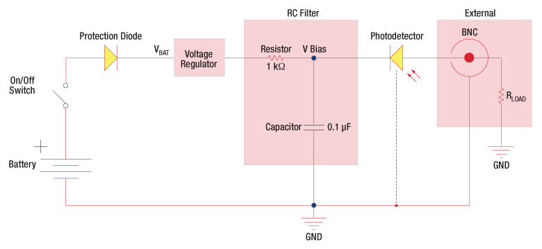
Figure 2: Reverse-Biased Circuit (DET Series Detectors)
The DET series detectors are modeled with the circuit depicted above. The detector is reverse biased to produce a linear response to the applied input light. The amount of photocurrent generated is based upon the incident light and wavelength and can be viewed on an oscilloscope by attaching a load resistance on the output. The function of the RC filter is to filter any high-frequency noise from the input supply that may contribute to a noisy output.
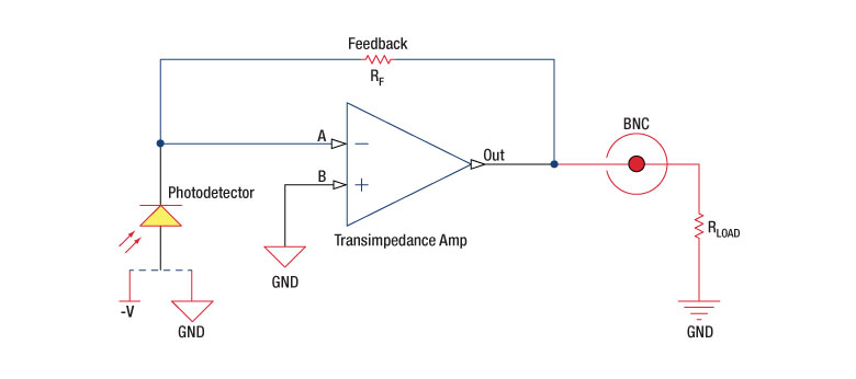
Figure 3: Amplified Detector Circuit
One can also use a photodetector with an amplifier for the purpose of achieving high gain. The user can choose whether to operate in Photovoltaic of Photoconductive modes. There are a few benefits of choosing this active circuit:
- Photovoltaic mode: The circuit is held at zero volts across the photodiode, since point A is held at the same potential as point B by the operational amplifier. This eliminates the possibility of dark current.
- Photoconductive mode: The photodiode is reversed biased, thus improving the bandwidth while lowering the junction capacitance. The gain of the detector is dependent on the feedback element (Rf). The bandwidth of the detector can be calculated using the following:
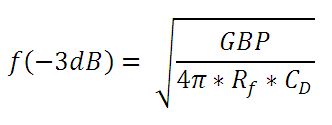
where GBP is the amplifier gain bandwidth product and CD is the sum of the junction capacitance and amplifier capacitance.
Effects of Chopping Frequency
The photoconductor signal will remain constant up to the time constant response limit. Many detectors, including PbS, PbSe, HgCdTe (MCT), and InAsSb, have a typical 1/f noise spectrum (i.e., the noise decreases as chopping frequency increases), which has a profound impact on the time constant at lower frequencies.
The detector will exhibit lower responsivity at lower chopping frequencies. Frequency response and detectivity are maximized for
![]()
| Posted Comments: | |
user
(posted 2023-09-21 12:29:35.553) Are you able to give me any more of the electrical characteristics of the VL5T0 such as the capacitance and noise? hchow
(posted 2023-09-25 03:48:28.0) Dear User, as this information is proprietary, I cannot disclose the specifications of the VL5T0 publicly. I will however reach out to you personally. Thank you. Mohsn.realtbzu
(posted 2017-12-25 04:27:19.91) Hi,I need output current of this photovoltaic for designig my project but in your datasheet wasn't Responsivity curve (A/W_landa)!
Would you please send me Resposivity curve inorder to find output current or say how can I find this electrical signal? wskopalik
(posted 2017-12-28 09:50:39.0) This is a response from Wolfgang at Thorlabs. Thank you very much for your inquiry.
The photovoltaic detector VML10T4 is specified with a current responsivity - width product of ≥ 0.15 A * mm * (1/W) at the optimal wavelength of 10.6µm. I have contacted you directly with further information about how to estimate the output current based on this specification. yt
(posted 2017-09-28 15:53:33.917) Hi!
Could you send us quotation VML10T4 with TEC amplifer like PDA10JT-EC type?
Best regards,
Y. T. Chae swick
(posted 2017-10-03 03:29:53.0) This is a response from Sebastian at Thorlabs. Thank you for the inquiry.
MCT detectors with integrated transimpedance amplifier (similar to PDA10JT) will be release soon.
I will contact you directly with further information. |
The following table lists Thorlabs' selection of photodiodes, photoconductive, and pyroelectric detectors. Item numbers in the same row contain the same detector element.
| Photodetector Cross Reference | ||||||
|---|---|---|---|---|---|---|
| Wavelength | Material | Unmounted Photodiode |
Mounted Photodiode |
Biased Detector |
Amplified Detector |
Amplified Detector, OEM Package |
| 200 - 1100 nm | Si | FDS010 | SM05PD2A SM05PD2B |
DET10A2 | PDA10A2 | - |
| Si | - | SM1PD2A | - | - | - | |
| 240 - 1170 nm | B-Si | - | - | DET20X2 | - | - |
| 320 - 1000 nm | Si | - | - | - | PDA8A2 | - |
| 320 - 1100 nm | Si | FD11A | SM05PD3A | - | PDF10A2 | - |
| Si | - a | - | DET100A2 a | PDA100A2 a | PDAPC2 a | |
| 340 - 1100 nm | Si | FDS10X10 | - | - | - | - |
| 350 - 1100 nm | Si | FDS100 FDS100-CAL b |
SM05PD1A SM05PD1B |
DET36A2 | PDA36A2 | PDAPC1 |
| Si | FDS1010 FDS1010-CAL b |
SM1PD1A SM1PD1B |
- | - | - | |
| 400 - 1000 nm | Si | - | - | - | PDA015A2 FPD310-FS-VIS FPD310-FC-VIS FPD510-FC-VIS FPD510-FS-VIS FPD610-FC-VIS FPD610-FS-VIS |
- |
| 400 - 1100 nm | Si | FDS015 c | - | - | - | - |
| Si | FDS025 c FDS02 d |
- | DET02AFC(/M) DET025AFC(/M) DET025A(/M) DET025AL(/M) |
- | - | |
| 400 - 1700 nm | Si & InGaAs | DSD2 | - | - | - | - |
| 500 - 1700 nm | InGaAs | - | - | DET10N2 | - | - |
| 0.6 - 16 µm | LiTaO3 | - | - | - | PDA13L2e | - |
| 750 - 1650 nm | InGaAs | - | - | - | PDA8GS | - |
| 800 - 1700 nm | InGaAs | FGA015 | - | - | PDA015C2 | - |
| InGaAs | FGA21 FGA21-CAL b |
SM05PD5A | DET20C2 | PDA20C2 PDA20CS2 |
- | |
| InGaAs | FGA01 c FGA01FC d |
- | DET01CFC(/M) | - | - | |
| InGaAs | FDGA05 c | - | - | PDA05CF2 | - | |
| InGaAs | - | - | DET08CFC(/M) DET08C(/M) DET08CL(/M) |
- | - | |
| InGaAs | - | - | - | PDF10C2 | - | |
| 800 - 1800 nm | Ge | FDG03 FDG03-CAL b |
SM05PD6A | DET30B2 | PDA30B2 | - |
| Ge | FDG50 | - | DET50B2 | PDA50B2 | - | |
| Ge | FDG05 | - | - | - | - | |
| 900 - 1700 nm | InGaAs | FGA10 | SM05PD4A | DET10C2 | PDA10CS2 | - |
| 900 - 2600 nm | InGaAs | FD05D | - | DET05D2 | - | - |
| FD10D | - | DET10D2 | PDA10D2 | - | ||
| 950 - 1650 nm | InGaAs | - | - | - | FPD310-FC-NIR FPD310-FS-NIR FPD510-FC-NIR FPD510-FS-NIR FPD610-FC-NIR FPD610-FS-NIR |
- |
| 1.0 - 5.8 µm | InAsSb | - | - | - | PDA10PT(-EC) | - |
| 2.0 - 8.0 µm | HgCdTe (MCT) | VML8T0 VML8T4 f |
- | - | PDAVJ8 | - |
| 2.0 - 10.6 µm | HgCdTe (MCT) | VML10T0 VML10T4 f |
- | - | PDAVJ10 | - |
| 2.7 - 5.0 µm | HgCdTe (MCT) | VL5T0 | - | - | PDAVJ5 | - |
| 2.7 - 5.3 µm | InAsSb | - | - | - | PDA07P2 | - |
 Photovoltaic Detector: 2.7 - 5 µm")
 Zoom
Zoom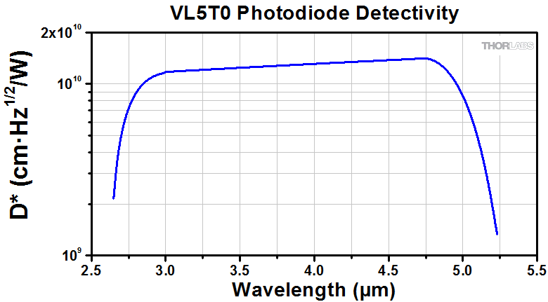
Click to Enlarge
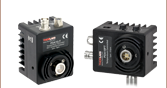
VL5T0 Photodiode Detectivity
- Wavelength Range: 2.7 - 5.0 µm
- TO-39 Package, Compatible with STO5S or STO5P Sockets
- Effective Sensor Area: 1 mm2 (1 mm x 1 mm)
- Acceptance Angle: 35°
- Single-Junction HgCdTe (MCT) Sensor
| Item # | Info | Optimization Wavelengtha |
Detectivity | TEC Stages |
Operating Temperature |
Time Constant |
Current Responsivity |
Resistance |
|---|---|---|---|---|---|---|---|---|
| VL5T0 | 5.0 µm | ≥9.0x10⁹ (cm·Hz1/2)/W | N/A | 27 °C | ≤120 ns | ≥1 A/W | ≥1 Ω·cm2 b |
 Photovoltaic Detectors: 2.0 - 8.0 µm")
 Zoom
Zoom
Click to Enlarge
VML8T0 and VML8T4 Photodiode Detectivity
- Wavelength Range 2.0 - 8.0 µm
- VML8T0: TO-39 Package, Compatible with STO5S or STO5P Sockets
- VML8T4: TO-8 Package with 4-Stage Thermoelectric Cooling (TEC)
- Effective Sensor Area: 1 mm2 (1 mm x 1 mm)
- Acceptance Angle: 35°
- Multi-Junction HgCdTe (MCT) Sensor
| Item # | Info | Optimization Wavelengtha |
Detectivity | TEC Stages |
Operating Temperature |
Time Constant |
Current Responsivity |
Resistance |
|---|---|---|---|---|---|---|---|---|
| VML8T0 | 8.0 µm | ≥3.0x10⁸ (cm·Hz1/2)/W | N/A | 27 °C | ≤4 ns | ≥0.04 A⋅mm/W | 50 to 300 Ω | |
| VML8T4 | 8.0 µm | ≥6.0x10⁹ (cm·Hz1/2)/W | Four | -78 °C | ≤4 ns | ≥0.20 A⋅mm/W | 500 to 1200 Ω |
 Photovoltaic Detectors: 2.0 - 10.6 µm")
 Zoom
Zoom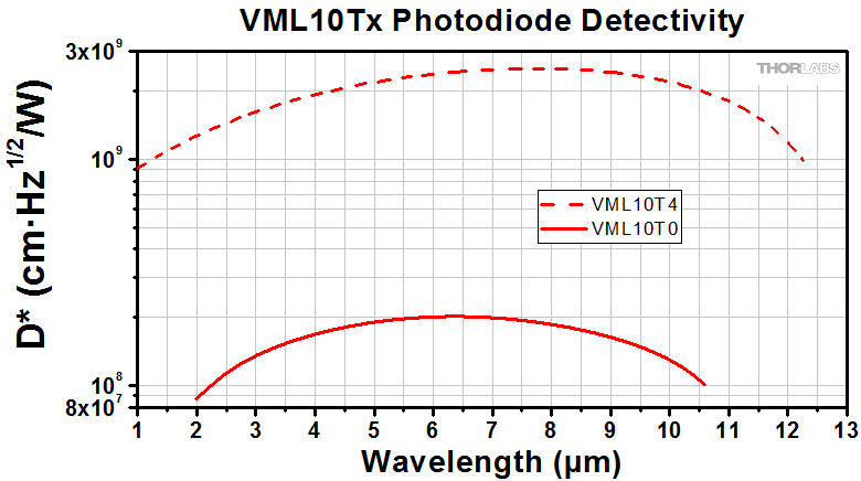
Click to Enlarge
VML10T0 and VML10T4 Photodiode Detectivity
- Wavelength Range 2.0 - 10.6 µm
- VML10T0: TO-39 Package, Compatible with STO5S or STO5P Sockets
- VML10T4: TO-8 Package with 4-Stage Thermoelectric Cooling (TEC)
- Effective Sensor Area: 1 mm2 (1 mm x 1 mm)
- Acceptance Angle: 35°
- Multi-Junction HgCdTe (MCT) Sensor
| Item # | Info | Optimization Wavelengtha |
Detectivity | TEC Stages |
Operating Temperature |
Time Constant |
Current Responsivity |
Resistance |
|---|---|---|---|---|---|---|---|---|
| VML10T0 | 10.6 µm | ≥1.0x10⁸ (cm·Hz1/2)/W | N/A | 27 °C | ≤1.5 ns | ≥0.01 A⋅mm/W | 20 to 150 Ω | |
| VML10T4 | 10.6 µm | ≥2.0x10⁹ (cm·Hz1/2)/W | Four | -78 °C | ≤3 ns | ≥0.15 A⋅mm/W | 150 to 500 Ω |