 Products Home / Detectors / Amplified Detectors / Si Amplified Detectors / Silicon and Black Silicon Free-Space Amplified Photodetectors, OEM Package
Silicon and Black Silicon Free-Space Amplified Photodetectors, OEM Package
- Wavelength Ranges from 200 nm to 1170 nm
- Maximum Bandwidths Up to 150 MHz
- Detector on Printed Circuit Board for OEM Applications
- Available in Fixed and Switchable Gain Configurations
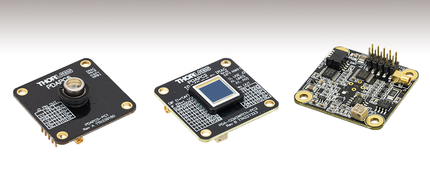
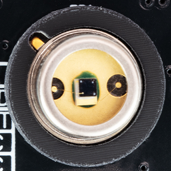
PDAPC5
Fixed Gain
200 - 1100 nm
150 MHz Max Bandwidth
PDAPC2
Switchable Gain
320 - 1100 nm
11 MHz Max Bandwidth
Front
Back


Please Wait

Click to Enlarge
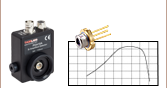
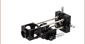
The OEM package free space amplified photodetectors can be integrated into a 30 mm cage system. In this example, a LA4148-B plano-convex lens mounted in a CP33 30 mm cage plate focuses light onto a PDAPC5 photodetector mounted with ER4 assembly rods.
| Item # | Wavelength Range | Bandwidth | Noise Equivalent Power (NEP) |
|---|---|---|---|
| Fixed Gain | |||
| PDAPC5 | 200 - 1100 nm | DC - 150 MHz | 29.2 pW/Hz1/2 |
| Switchable Gain | |||
| PDAPC10a | 240 - 1170 nm | DC - 11 MHzb | 3.27 - 60 pW/Hz1/2 |
| PDAPC2a | 320 - 1100 nm | DC - 11 MHzb | 2.67 - 71.7 pW/Hz1/2 |
| PDAPC1a | 350 - 1100 nm | DC - 12 MHzb | 3.25 - 75.7 pW/Hz1/2 |
Features
- One Fixed Gain Model Available for UV, Visible, and NIR:
- PDAPC5: 200 to 1100 nm
- Three Switchable Gain Models Available for UV, Visible, and NIR:
- PDAPC10: 240 to 1170 nm
- PDAPC2: 320 to 1100 nm
- PDAPC1: 350 to 1100 nm
- Low-Noise Amplification with Fixed or Switchable Gain
- 50 Ω and Higher Load Impedances
- Free-Space Optical Coupling
- Output Accessible via On-Board Header Pins and Female MMCX Connector
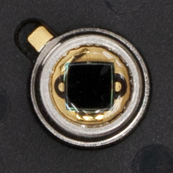
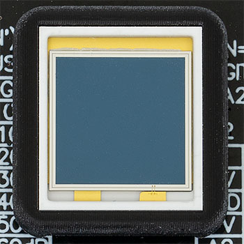
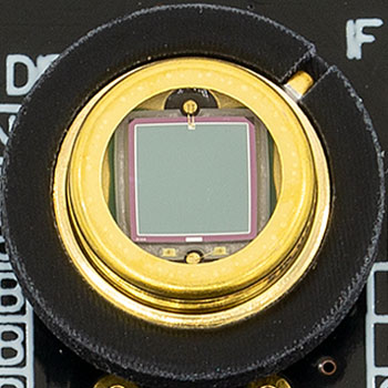
We offer a selection of Silicon (Si) and Black Silicon (b-Si) Free-Space Amplified Photodetectors that are sensitive to light from the UV to the near infrared. When compared to regular silicon, the responsivity of black silicon changes linearly with wavelength from approximately 400 - 1000 nm.
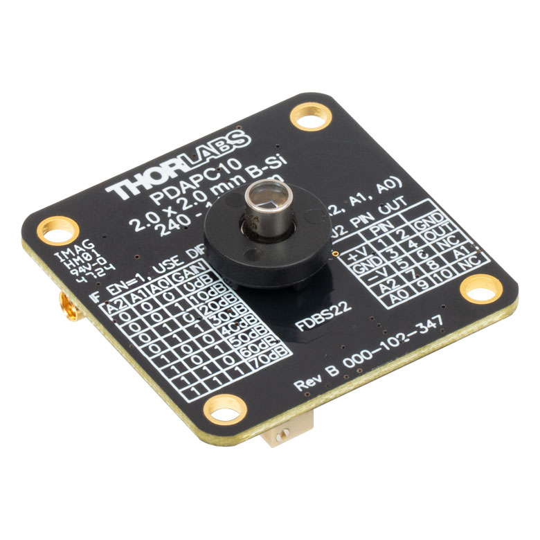
These amplified photodetectors feature a built-in low-noise transimpedance amplifier (TIA) and either fixed gain or switchable gain with eight gain settings. Gain can be adjusted via on-board header pins or manually through four DIP switches. The fixed gain model has a 150 MHz bandwidth, and the switchable gain models have a maximum bandwidth of 11 or 12 MHz.
The photodetectors are capable of driving loads from 50 Ω to Hi-Z with the output being accessible through a jumper or an MMCX connector on the rear of the printed circuit board (PCB). Each detector PCB has four Ø3.2 mm (0.12") through holes on a 30 mm square grid for compatibility with our 30 mm cage system or mounting in custom housings and devices.
Power Supply
A ±12 V linear power supply that supports input voltages of 100, 120, and 230 VAC is available for purchase separately below. Before connecting the power supply to mains voltage, ensure that the mains voltage switch on the power supply module is set to the proper voltage range. The power supply should always be powered up using the power switch on the power supply itself. Hot plugging the unit is not recommended.
| Performance Specifications | |||||||
|---|---|---|---|---|---|---|---|
| Item # | Wavelength | Bandwidth | Rise Time | Peak Responsivity |
Noise Equivalent Power (NEP)a |
Active Area | Operating Temperature Range |
| Fixed Gain | |||||||
| PDAPC5b | 200 - 1100 nm | DC - 150 MHz | 2.3 ns | 0.44 A/W @ 730 nm | 29.2 pW/Hz1/2 | 0.8 mm2 (Ø1.0 mm) | 10 to 40 °C |
| Switchable Gain | |||||||
| PDAPC10 | 240 - 1170 nm | DC - 11 MHzc | N/Ad | 0.73 A/W @ 1010 nm | 3.27 - 60 pW/Hz1/2 | 4 mm2 (2 mm x 2 mm) | 10 to 40 °C |
| PDAPC2b | 320 - 1100 nm | DC - 11 MHzc | N/Ad | 0.72 A/W @ 960 nm | 2.67 - 71.7 pW/Hz1/2 | 100 mm2 (10 mm x 10 mm) | |
| PDAPC1b | 350 - 1100 nm | DC - 12 MHzc | N/Ad | 0.65 A/W @ 970 nm | 3.25 - 75.7 pW/Hz1/2 | 13 mm2 (3.6 mm x 3.6 mm) | |
| Gain Specifications | |||||||||
|---|---|---|---|---|---|---|---|---|---|
| Item # | Gain Step (dB) |
Gain w/ Hi-Z Load |
Gain w/ 50 Ω Load |
Bandwidtha | Noise (RMS) |
Noise Equivalent Power (NEP)b | Offset (±) | Output Voltage w/ Hi-Z Load |
Output Voltage w/ 50 Ω Load |
| Fixed Gain | |||||||||
| PDAPC5 | N/A | 10 kV/A ± 2% | 5 kV/A ± 2% | 150 MHz | 1.5 mV | 29.2 pW/Hz1/2 | 10 mV Max | 0 - 10 V | 0 - 5 V |
| Switchable Gain | |||||||||
| PDAPC10 | 0 | 1.51 kV/A ± 2% | 0.75 kV/A ± 2% | 11 MHz | 234 µV | 60 pW/Hz1/2 | 8 mV (12 mV Max) | 0 - 10 V | 0 - 5 V |
| 10 | 4.75 kV/A ± 2% | 2.38 kV/A ± 2% | 1.3 MHz | 238 µV | 6.15 pW/Hz1/2 | ||||
| 20 | 15 kV/A ± 2% | 7.5 kV/A ± 2% | 1.4 MHz | 249 µV | 3.27 pW/Hz1/2 | ||||
| 30 | 47.5 kV/A ± 2% | 23.8 kV/A ± 2% | 430 kHz | 246 µV | 3.9 pW/Hz1/2 | ||||
| 40 | 151 kV/A ± 2% | 75 kV/A ± 2% | 110 kHz | 245 µV | 3.36 pW/Hz1/2 | ||||
| 50 | 475 kV/A ± 2% | 238 kV/A ± 2% | 40 kHz | 250 µV | 5.95 pW/Hz1/2 | ||||
| 60 | 1.5 MV/A ± 5% | 750 kV/A ± 5% | 11 kHz | 253 µV | 7.52 pW/Hz1/2 | ||||
| 70 | 4.75 MV/A ± 5% | 2.38 MV/A ± 5% | 4 kHz | 265 µV | 5.01 pW/Hz1/2 | ||||
| PDAPC2 | 0 | 1.51 kV/A ± 2% | 0.75 kV/A ± 2% | 11 MHz | 268 µV | 71.7 pW/Hz1/2 | 8 mV (12 mV Max) | ||
| 10 | 4.75 kV/A ± 2% | 2.38 kV/A ± 2% | 1.4 MHz | 195 µV | 6.75 pW/Hz1/2 | ||||
| 20 | 15 kV/A ± 2% | 7.5 kV/A ± 2% | 800 kHz | 219 µV | 3.36 pW/Hz1/2 | ||||
| 30 | 47.5 kV/A ± 2% | 23.8 kV/A ± 2% | 260 kHz | 222 µV | 2.83 pW/Hz1/2 | ||||
| 40 | 151 kV/A ± 2% | 75 kV/A ± 2% | 90 kHz | 229 µV | 2.67 pW/Hz1/2 | ||||
| 50 | 475 kV/A ± 2% | 238 kV/A ± 2% | 28 kHz | 271 µV | 4.2 pW/Hz1/2 | ||||
| 60 | 1.5 MV/A ± 5% | 750 kV/A ± 5% | 9 kHz | 423 µV | 6.24 pW/Hz1/2 | ||||
| 70 | 4.75 MV/A ± 5% | 2.38 MV/A ± 5% | 3 kHz | 1.22 mV | 7.88 pW/Hz1/2 | ||||
| PDAPC1 | 0 | 1.51 kV/A ± 2% | 0.75 kV/A ± 2% | 12 MHz | 258 µV | 75.7 pW/Hz1/2 | 8 mV (12 mV Max) | ||
| 10 | 4.75 kV/A ± 2% | 2.38 kV/A ± 2% | 1.6 MHz | 192 µV | 5.8 pW/Hz1/2 | ||||
| 20 | 15 kV/A ± 2% | 7.5 kV/A ± 2% | 1 MHz | 207 µV | 3.4 pW/Hz1/2 | ||||
| 30 | 47.5 kV/A ± 2% | 23.8 kV/A ± 2% | 260 kHz | 211 µV | 3.4 pW/Hz1/2 | ||||
| 40 | 150 kV/A ± 2% | 75 kV/A ± 2% | 90 kHz | 214 µV | 3.25 pW/Hz1/2 | ||||
| 50 | 475 kV/A ± 2% | 238 kV/A ± 2% | 28 kHz | 234 µV | 3.69 pW/Hz1/2 | ||||
| 60 | 1.5 MV/A ± 5% | 750 kV/A ± 5% | 9 kHz | 277 µV | 4 pW/Hz1/2 | ||||
| 70 | 4.75 MV/A ± 5% | 2.38 MV/A ± 5% | 3 kHz | 388 µV | 4.29 pW/Hz1/2 | ||||
J2 Header Pins |
|||||||||||||||||||||||||
 |
|
||||||||||||||||||||||||
DIP Switches
|
||||||||||
|
Gain Settingsa
|
||||||||||||||||||||||||||||||||||||
|
Female MMCX Connector
|
 |
| 0 to 5 V (50 Ω) 0 to 10 V (Hi-Z) |
Photodiode Tutorial
Theory of Operation
A junction photodiode is an intrinsic device that behaves similarly to an ordinary signal diode, but it generates a photocurrent when light is absorbed in the depleted region of the junction semiconductor. A photodiode is a fast, highly linear device that exhibits high quantum efficiency and may be used in a variety of different applications.
It is necessary to be able to correctly determine the level of the output current to expect and the responsivity based upon the incident light. Depicted in Figure 100A is a junction photodiode model with basic discrete components to help visualize the main characteristics and gain a better understanding of the operation of Thorlabs' photodiodes.
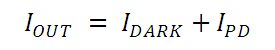
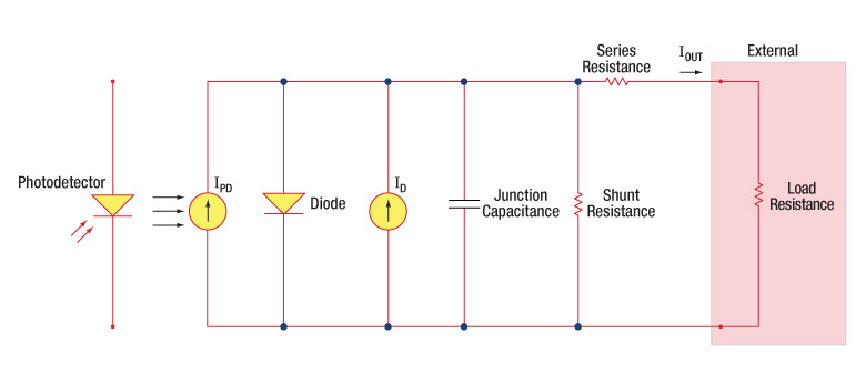
Figure 100A Photodiode Model
Photodiode Terminology
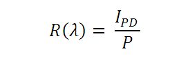
Responsivity
The responsivity of a photodiode can be defined as a ratio of generated photocurrent (IPD) to the incident light power (P) at a given wavelength:
Modes of Operation (Photoconductive vs. Photovoltaic)
A photodiode can be operated in one of two modes: photoconductive (reverse bias) or photovoltaic (zero-bias). Mode selection depends upon the application's speed requirements and the amount of tolerable dark current (leakage current).
Photoconductive
In photoconductive mode, an external reverse bias is applied, which is the basis for our DET series detectors. The current measured through the circuit indicates illumination of the device; the measured output current is linearly proportional to the input optical power. Applying a reverse bias increases the width of the depletion junction producing an increased responsivity with a decrease in junction capacitance and produces a very linear response. Operating under these conditions does tend to produce a larger dark current, but this can be limited based upon the photodiode material. (Note: Our DET detectors are reverse biased and cannot be operated under a forward bias.)
Photovoltaic
In photovoltaic mode the photodiode is zero biased. The flow of current out of the device is restricted and a voltage builds up. This mode of operation exploits the photovoltaic effect, which is the basis for solar cells. The amount of dark current is kept at a minimum when operating in photovoltaic mode.
Dark Current
Dark current is leakage current that flows when a bias voltage is applied to a photodiode. When operating in a photoconductive mode, there tends to be a higher dark current that varies directly with temperature. Dark current approximately doubles for every 10 °C increase in temperature, and shunt resistance tends to double for every 6 °C rise. Of course, applying a higher bias will decrease the junction capacitance but will increase the amount of dark current present.
The dark current present is also affected by the photodiode material and the size of the active area. Silicon devices generally produce low dark current compared to germanium devices which have high dark currents. Table 100B lists several photodiode materials and their relative dark currents, speeds, spectral ranges, and costs.
| Table 100B Photodiode Materials | ||||
|---|---|---|---|---|
| Material | Dark Current | Speed | Spectral Range | Cost |
| Silicon (Si) | Low | High Speed | Visible to NIR | Low |
| Black Silicon (B-Si) | Low | Medium Speeda | Visible to NIR | Moderate |
| Germanium (Ge) | High | Low Speed | NIR | Low |
| Indium Gallium Arsenide (InGaAs) | Low | High Speed | NIR | Moderate |
| Indium Arsenide Antimonide (InAsSb) | High | Low Speed | NIR to MIR | High |
| Extended Range Indium Gallium Arsenide (InGaAs) | High | High Speed | NIR | High |
| Mercury Cadmium Telluride (MCT, HgCdTe) | High | Low Speed | NIR to MIR | High |
Junction Capacitance
Junction capacitance (Cj) is an important property of a photodiode as this can have a profound impact on the photodiode's bandwidth and response. It should be noted that larger diode areas encompass a greater junction volume with increased charge capacity. In a reverse bias application, the depletion width of the junction is increased, thus effectively reducing the junction capacitance and increasing the response speed.
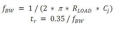
Bandwidth and Response
A load resistor will react with the photodetector junction capacitance to limit the bandwidth. For best frequency response, a 50 Ω terminator should be used in conjunction with a 50 Ω coaxial cable. The bandwidth (fBW) and the rise time response (tr) can be approximated using the junction capacitance (Cj) and the load resistance (RLOAD):
Noise Equivalent Power
The noise equivalent power (NEP) is the input signal power that results in a signal-to-noise ratio (SNR) of 1 in a 1 Hz output bandwidth. This is useful, as the NEP determines the ability of the detector to detect low level light. In general, the NEP increases with the active area of the detector and is given by the following equation:
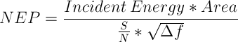
Here, S/N is the Signal to Noise Ratio, Δf is the Noise Bandwidth, and Incident Energy has units of W/cm2. For more information on NEP, please see Thorlabs' Noise Equivalent Power White Paper.
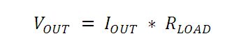
Terminating Resistance
A load resistance is used to convert the generated photocurrent into a voltage (VOUT) for viewing on an oscilloscope:
Depending on the type of the photodiode, load resistance can affect the response speed. For maximum bandwidth, we recommend using a 50 Ω coaxial cable with a 50 Ω terminating resistor at the opposite end of the cable. This will minimize ringing by matching the cable with its characteristic impedance. If bandwidth is not important, you may increase the amount of voltage for a given light level by increasing RLOAD. In an unmatched termination, the length of the coaxial cable can have a profound impact on the response, so it is recommended to keep the cable as short as possible.
Shunt Resistance
Shunt resistance represents the resistance of the zero-biased photodiode junction. An ideal photodiode will have an infinite shunt resistance, but actual values may range from the order of ten Ω to thousands of MΩ and is dependent on the photodiode material. For example, and InGaAs detector has a shunt resistance on the order of 10 MΩ while a Ge detector is in the kΩ range. This can significantly impact the noise current on the photodiode. For most applications, however, the high resistance produces little effect and can be ignored.
Series Resistance
Series resistance is the resistance of the semiconductor material, and this low resistance can generally be ignored. The series resistance arises from the contacts and the wire bonds of the photodiode and is used to mainly determine the linearity of the photodiode under zero bias conditions.
Common Operating Circuits
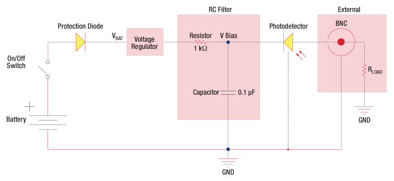
Figure 100C Reverse-Biased Circuit (DET Series Detectors)
The DET series detectors are modeled with the circuit depicted in Figure 100C. The detector is reverse biased to produce a linear response to the applied input light. The amount of photocurrent generated is based upon the incident light and wavelength and can be viewed on an oscilloscope by attaching a load resistance on the output. The function of the RC filter is to filter any high-frequency noise from the input supply that may contribute to a noisy output.
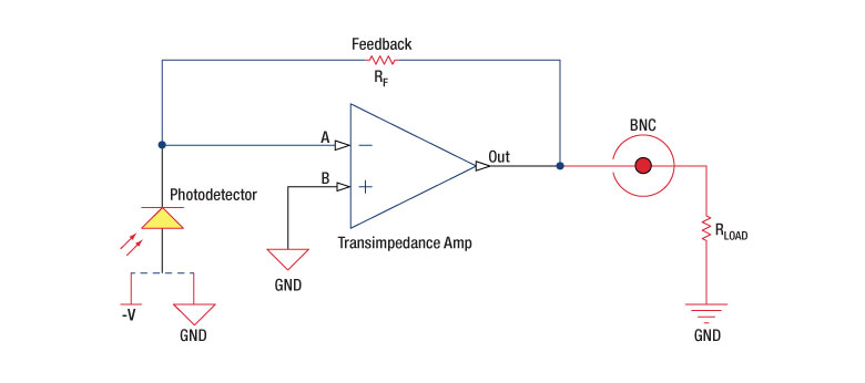
Figure 100D Amplified Detector Circuit
One can also use a photodetector with an amplifier for the purpose of achieving high gain. The user can choose whether to operate in Photovoltaic of Photoconductive modes. There are a few benefits of choosing this active circuit:
- Photovoltaic mode: The circuit is held at zero volts across the photodiode, since point A is held at the same potential as point B by the operational amplifier. This eliminates the possibility of dark current.
- Photoconductive mode: The photodiode is reversed biased, thus improving the bandwidth while lowering the junction capacitance. The gain of the detector is dependent on the feedback element (Rf). The bandwidth of the detector can be calculated using the following:
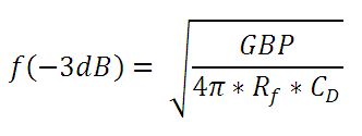
where GBP is the amplifier gain bandwidth product and CD is the sum of the junction capacitance and amplifier capacitance.
Effects of Chopping Frequency
The photoconductor signal will remain constant up to the time constant response limit. Many detectors, including PbS, PbSe, HgCdTe (MCT), and InAsSb, have a typical 1/f noise spectrum (i.e., the noise decreases as chopping frequency increases), which has a profound impact on the time constant at lower frequencies.
The detector will exhibit lower responsivity at lower chopping frequencies. Frequency response and detectivity are maximized for
![]()
Pulsed Laser Emission: Power and Energy Calculations

Determining whether emission from a pulsed laser is compatible with a device or application can require referencing parameters that are not supplied by the laser's manufacturer. When this is the case, the necessary parameters can typically be calculated from the available information. Calculating peak pulse power, average power, pulse energy, and related parameters can be necessary to achieve desired outcomes including:
- Protecting biological samples from harm.
- Measuring the pulsed laser emission without damaging photodetectors and other sensors.
- Exciting fluorescence and non-linear effects in materials.
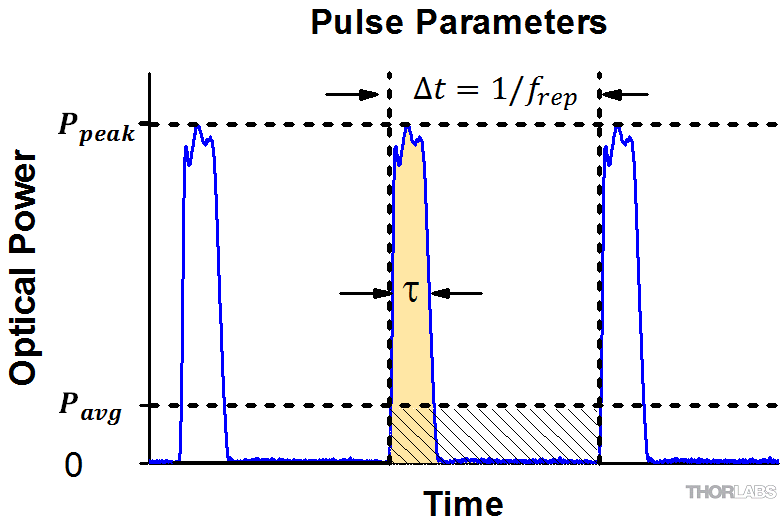
Pulsed laser radiation parameters are illustrated in Figure 170A and described in Table 170B. For quick reference, a list of equations is provided below. The document available for download provides this information, as well as an introduction to pulsed laser emission, an overview of relationships among the different parameters, and guidance for applying the calculations.
|
Equations: |
||||
 |
and |  |
||
 |
||||
 |
||||
 |
||||
Peak power and average power calculated from each other: |
||||
 |
and |  |
||
| Peak power calculated from average power and duty cycle*: | ||||
 |
*Duty cycle ( ) is the fraction of time during which there is laser pulse emission. ) is the fraction of time during which there is laser pulse emission. |
|||
Click to Enlarge
Figure 170A Parameters used to describe pulsed laser emission are indicated in this plot and described in Table 170B. Pulse energy (E) is the shaded area under the pulse curve. Pulse energy is, equivalently, the area of the diagonally hashed region.
| Table 170B Pulse Parameters | |||||
|---|---|---|---|---|---|
| Parameter | Symbol | Units | Description | ||
| Pulse Energy | E | Joules [J] | A measure of one pulse's total emission, which is the only light emitted by the laser over the entire period. The pulse energy equals the shaded area, which is equivalent to the area covered by diagonal hash marks. | ||
| Period | Δt | Seconds [s] | The amount of time between the start of one pulse and the start of the next. | ||
| Average Power | Pavg | Watts [W] | The height on the optical power axis, if the energy emitted by the pulse were uniformly spread over the entire period. | ||
| Instantaneous Power | P | Watts [W] | The optical power at a single, specific point in time. | ||
| Peak Power | Ppeak | Watts [W] | The maximum instantaneous optical power output by the laser. | ||
| Pulse Width |  |
Seconds [s] | A measure of the time between the beginning and end of the pulse, typically based on the full width half maximum (FWHM) of the pulse shape. Also called pulse duration. | ||
| Repetition Rate | frep | Hertz [Hz] | The frequency with which pulses are emitted. Equal to the reciprocal of the period. | ||
Example Calculation:
Is it safe to use a detector with a specified maximum peak optical input power of 75 mW to measure the following pulsed laser emission?
- Average Power: 1 mW
- Repetition Rate: 85 MHz
- Pulse Width: 10 fs
The energy per pulse:

seems low, but the peak pulse power is:

It is not safe to use the detector to measure this pulsed laser emission, since the peak power of the pulses is >5 orders of magnitude higher than the detector's maximum peak optical input power.
| Posted Comments: | |
Thomas Le Deun
(posted 2024-08-22 06:50:22.48) Hello,
I just bought 2 PDAPC2, it is very convenient and useful. However I think it would be even better if the 4 holes were 4mm or 6mm in diameter, so the entire product could slide on rods so we could easily adjust the position on cage systems.
Let me know if this is something you could provide, we would be very interested!
Best regards,
Thomas Le Deun ksosnowski
(posted 2024-08-27 04:06:04.0) Hello Thomas, thank you for reaching out to us with this feedback. This is an interesting idea and I have reached out directly to discuss this potential customization further. Ingo Schilling
(posted 2024-01-16 16:06:45.123) Hello
I can't find any information about the maximum optical input power. There is the peak responsivity but then I still need the max current. Can you help? ksosnowski
(posted 2024-01-17 10:43:05.0) Hello Ingo, thanks for reaching out to Thorlabs. PDAPC1 uses our FDS100 photodiode which has a max photocurrent limit of 5mA. For considering the max power on the amplified PDA series you will also want to ensure that the output voltage is less than the maximum rating for the device as this is the point of amplifier saturation. Vita Ivanova
(posted 2023-03-02 09:16:53.407) We need PDAPC2 - Si Switchable Gain Detector on PCB, 320 - 1100 nm, 11 MHz BW, 100 mm² for use in the laboratory of Igor Sikorskyi Kyiv Polytechnical Institute, Ukraine.
Are discounts possible for 1 detector? ksosnowski
(posted 2023-03-02 10:06:28.0) Hello Vita, thanks for reaching out to Thorlabs. There is not any standard discount we have for a single unit like this, however you can read our full discount policy here: https://www.thorlabs.com/discountpolicy.cfm Howard Yoon
(posted 2022-10-18 17:08:05.043) Can these devices be powered by +- 9 V instead of +- 12 V? ksosnowski
(posted 2022-10-19 09:59:22.0) Thanks for reaching out to Thorlabs. The PDAPCx OEM boards are only designed to operate at 12V. We recommend using our LDS12B as a proper dual rail power supply. Using 9V supply the amplifier performance would change as well as the photodiode bias. Using higher voltages can damage the amplifier or photodiode. Tobias Meyer
(posted 2022-09-27 12:29:31.95) Hi, is there anything comparable to PDCAP1/PDCAP2 and capable of handling larger temperatures up to 80°C? ksosnowski
(posted 2022-09-28 05:04:52.0) Thanks for reaching out to Thorlabs. At higher temperatures the photodiode and amplifier performances can shift, and some components like connectors/cabling are not rated for this high of temperature. Unfortunately we do not currently have similar detectors with a higher operating temperature range. If the high temperature is due to thermal radiation from the light source, you may be able to consider using our Hot Mirrors like M254H45 to reflect this from the sensor. Marco Menchetti
(posted 2022-09-05 13:15:15.437) Hi,
Is it possible to modify the board so that two PD can operate in differential mode?
Regards
Marco cdolbashian
(posted 2022-09-07 03:56:25.0) Thank you for reaching out to us with this inquiry. With the appropriate background in electronics, it is possible to do such a modification, though this is not something we can directly support. For differential measurements in an OEM style package, we recommend looking at the offerings we have here: https://www.thorlabs.com/navigation.cfm?guide_id=2120 Sayyed Kamal
(posted 2022-04-27 17:11:05.58) Question about the gain setting inputs. I am trying to control the gain via an MCU. Is the logic high threshold >3.5V? cdolbashian
(posted 2022-05-04 04:50:03.0) Thank you for reaching out to us with this inquiry. Regarding the gain inputs on the J2 header for PDAPC1, the High-level input voltage is 3.85V minimum, rather than 3.5V. |
The following table lists Thorlabs' selection of photodiodes, photoconductive, and pyroelectric detectors. Item numbers in the same row contain the same detector element.
| Photodetector Cross Reference | ||||||
|---|---|---|---|---|---|---|
| Wavelength | Material | Unmounted Photodiode |
Mounted Photodiode |
Biased Detector |
Amplified Detector |
Amplified Detector, OEM Package |
| 200 - 1100 nm | Si | FDS010 | SM05PD2A SM05PD2B |
DET10A2 | PDA10A2 | PDAPC5 |
| Si | - | SM1PD2A | - | - | - | |
| 240 - 1170 nm | Black Si | FDBS11 | SM05PD9A | - | - | - |
| Black Si | FDBS22 | SM05PD8A | DET20X2 | PDA20X2 | PDAPC10 | |
| Black Si | FDBS25 | - | - | - | - | |
| 320 - 1000 nm | Si | - | - | - | PDA8A2 | - |
| 320 - 1100 nm | Si | FD11A | SM05PD3A | - | PDF10A2 | - |
| Si | - a | - | DET100A2 a | PDA100A2 a | PDAPC2 a | |
| 340 - 1100 nm | Si | FDS10X10 | - | - | - | - |
| 350 - 1100 nm | Si | FDS100 FDS100-CAL b |
SM05PD1A SM05PD1B |
DET36A2 | PDA36A2 | PDAPC1 |
| Si | FDS1010 FDS1010-CAL b |
SM1PD1A SM1PD1B |
- | - | - | |
| 400 - 1000 nm | Si | - | - | - | PDA015A2 FPD310-FS-VIS FPD310-FC-VIS FPD510-FC-VIS FPD510-FS-VIS FPD610-FC-VIS FPD610-FS-VIS |
- |
| 400 - 1100 nm | Si | FDS015 c | - | - | - | - |
| Si | FDS025 c FDS02 d |
- | DET02AFC ( /M ) DET025AFC ( /M ) DET025A ( /M ) DET025AL ( /M ) |
- | - | |
| 400 - 1700 nm | Si & InGaAs | DSD2 | - | - | - | - |
| 500 - 1700 nm | InGaAs | - | - | DET10N2 | - | - |
| 0.6 - 16 µm | LiTaO 3 | - | - | - | PDA13L2 e | - |
| 750 - 1650 nm | InGaAs | - | - | - | PDA8GS | - |
| 800 - 1700 nm | InGaAs | FGA015 | - | - | PDA015C2 | - |
| InGaAs | FGA21 FGA21-CAL b |
SM05PD5A | DET20C2 | PDA20C2 PDA20CS2 |
- | |
| InGaAs | FGA01 c FGA01FC d |
- | DET01CFC ( /M ) | - | - | |
| InGaAs | FDGA05 c | - | - | PDA05CF2 | PDAPC6 | |
| InGaAs | - | - | DET08CFC ( /M ) DET08C ( /M ) DET08CL ( /M ) |
- | - | |
| InGaAs | - | - | - | PDF10C2 | - | |
| 800 - 1800 nm | Ge | FDG03 FDG03-CAL b |
SM05PD6A | DET30B2 | PDA30B2 | - |
| Ge | FDG50 | - | DET50B2 | PDA50B2 | PDAPC8 | |
| Ge | FDG05 | - | - | - | - | |
| 900 - 1700 nm | InGaAs | FGA10 | SM05PD4A | DET10C2 | PDA10CS2 | - |
| 900 - 2600 nm | InGaAs | FD05D | - | DET05D2 | - | - |
| FD10D | - | DET10D2 | PDA10D2 | PDAPC7 | ||
| 950 - 1650 nm | InGaAs | - | - | - | FPD310-FC-NIR FPD310-FS-NIR FPD510-FC-NIR FPD510-FS-NIR FPD610-FC-NIR FPD610-FS-NIR |
- |
| 1.0 - 5.8 µm | InAsSb | - | - | - | PDA10PT ( -EC ) | - |
| 2.0 - 8.0 µm | HgCdTe (MCT) | VML8T0 VML8T4 f |
- | - | PDAVJ8 | - |
| 2.0 - 10.6 µm | HgCdTe (MCT) | VML10T0 VML10T4 f |
- | - | PDAVJ10 | - |
| 2.7 - 5.0 µm | HgCdTe (MCT) | VL5T0 | - | - | PDAVJ5 | - |
| 2.7 - 5.3 µm | InAsSb | - | - | - | PDA07P2 | PDAPC9 |
| Item #a | Package Featuresb |
Wavelength Range |
Bandwidth Rangec |
Gain | Noise Equivalent Power (NEP)d | Typical Performance Graphs |
Active Area (Click Link for Image) |
Operating Temperature Range |
|
|---|---|---|---|---|---|---|---|---|---|
| Hi-Z Load | 50 Ω Load | ||||||||
| PDAPC5e | 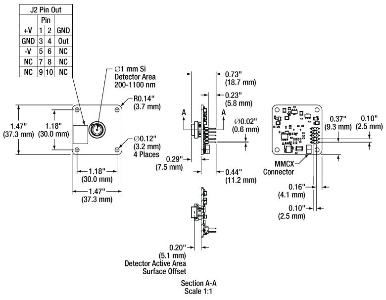 |
200 - 1100 nm | DC - 150 MHz | 10 kV/A | 5 kV/A | 29.2 pW/Hz1/2 | 0.8 mm2 (Ø1.0 mm) | 10 to 40 °C | |
| Item #a | Package Featuresb |
Wavelength Range |
Bandwidth Rangec |
Gain | Noise Equivalent Power (NEP)d | Typical Performance Graphs |
Active Area (Click Link for Image) |
Operating Temperature Range |
|
|---|---|---|---|---|---|---|---|---|---|
| Hi-Z Load | 50 Ω Load | ||||||||
| PDAPC10e | 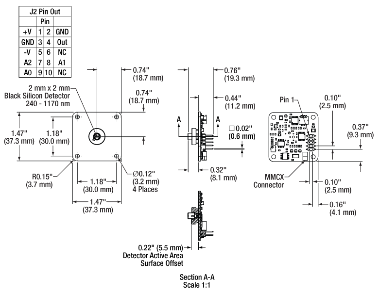 |
240 - 1170 nm | DC - 11 MHzf | 1.51 kV/A - 4.75 MV/A | 0.75 kV/A - 2.38 MV/A | 3.27 - 60 pW/Hz1/2 | 4 mm2 (2 mm x 2 mm) |
10 to 40 °C | |
| Item #a | Package Featuresb |
Wavelength Range |
Bandwidth Rangec |
Gain | Noise Equivalent Power (NEP)d | Typical Performance Graphs |
Active Area (Click Link for Image) |
Operating Temperature Range |
|
|---|---|---|---|---|---|---|---|---|---|
| Hi-Z Load | 50 Ω Load | ||||||||
| PDAPC2e | 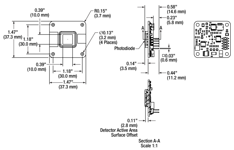 |
320 - 1100 nm | DC - 11 MHzf | 1.51 kV/A - 4.75 MV/A | 0.75 kV/A - 2.38 MV/A | 2.67 - 71.7 pW/Hz1/2 | 100 mm2 (10 mm x 10 mm) |
10 to 40 °C | |
| PDAPC1e | 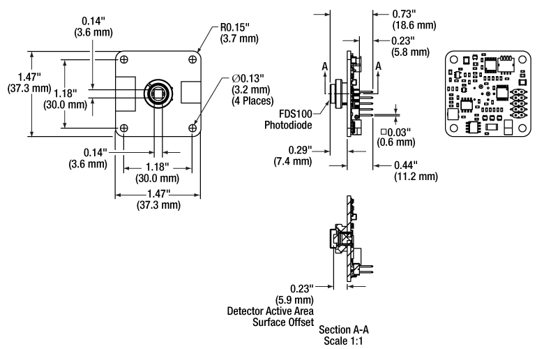 |
350 - 1100 nm | DC - 12 MHzf | 1.51 kV/A - 4.75 MV/A | 0.75 kV/A - 2.38 MV/A | 3.25 - 75.7 pW/Hz1/2 | 13 mm2 |
10 to 40 °C | |

 Zoom
Zoom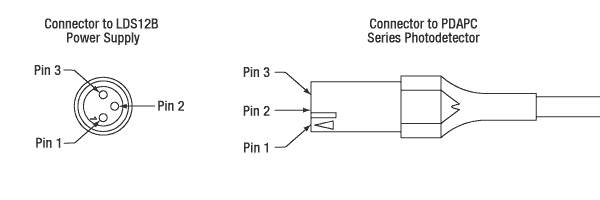
Click to Enlarge
Pin Diagram for the Included Cable
| Pin # | Assignment |
|---|---|
| 1 | +12 V |
| 2 | GND |
| 3 | -12 V |
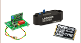
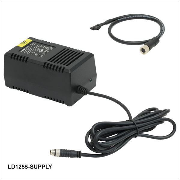
- Power Supply (Item # LDS12B) and Cable for Use with PDAPC Series Photodetectors
- 3 Pin Cable Output Connects to J2 Jumper on Detector Board
- ±12 VDC Output
- Switchable Input Voltage: 100 V, 120 V, or 230 V
The LD1255-SUPPLY Bundle includes the LDS12B Power Supply and the appropriate cable to connect to PDAPC Series Photo detectors (available above). A switch on the power supply box enables the user to choose a 100 V, 120 V, or 230 V input voltage. The cable is able to transmit ±12 VDC from the power supply to the photodetector. The included cable can be ordered separately from the power supply by contacting Tech Support.

 Zoom
Zoom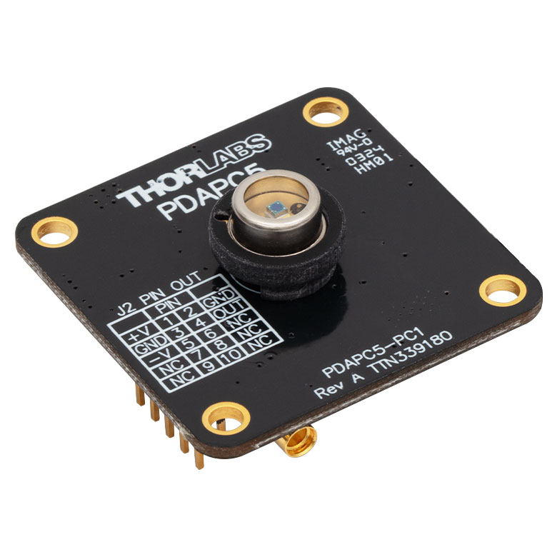
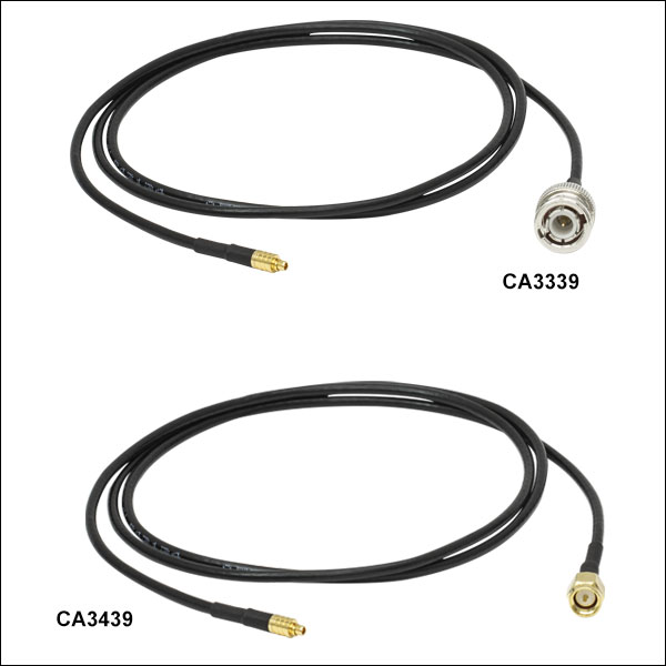
- Optional Cables for Output of PDAPC Series Photodetectors
- MMCX Male Connector to BNC or SMA Male Connector
- DC - 6 GHz Frequency Range
- 50 Ω Normal Impedance
- 170 V Max Operating Voltage
These cables convert the MMCX output of the photodetectors sold above to BNC or SMA male connectors. The CA3339 (1 m long) and CA3272 (1.8 m long) cables feature a male BNC termination while the CA3439 (1 m long) has a male SMA termination.