 Products Home
Optical Coatings
- State-of-the-Art, In-House Coating Lab
- Broad Range of Coating Capabilities on a Wide Variety of Substrates
- Textured Surface Capabilities for Broadband Antireflection Performance

Please Wait
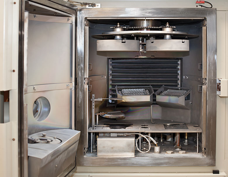
Click to Enlarge
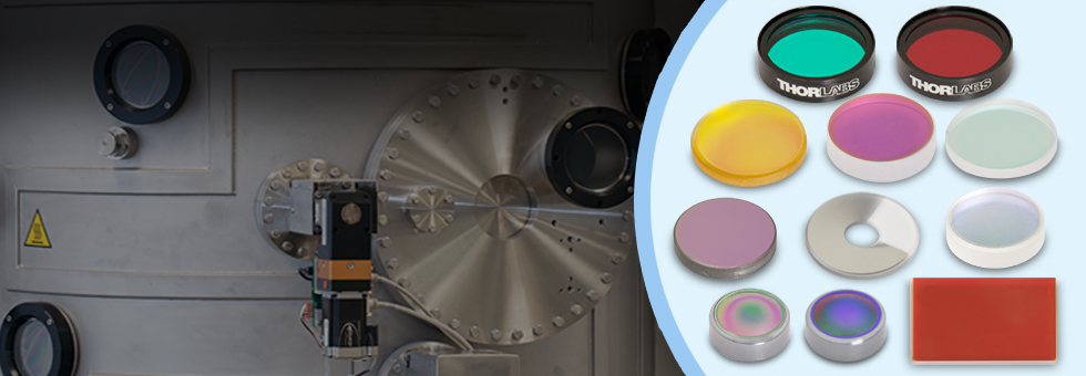
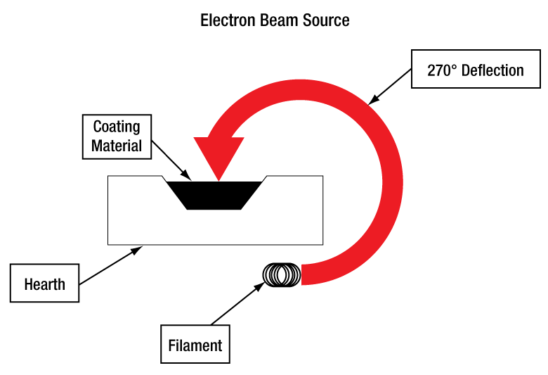
Interior of an E-Beam Deposition Chamber

Thorlabs' Coating Capabilities
Thorlabs' state-of-the-art, in-house, optical coating department provides us with coating capabilities ranging from metal coatings and antireflective coatings to cutting edge Ion Beam Sputtered (IBS), Radio Frequency (RF) Magnetron Sputtered, and Plasma Assisted coatings. This full-scale facility not only allows us to produce large numbers of our catalog optics in house but also expands our ability to manufacture custom-coated optics to suit a variety of customer needs.
Several coating chambers are outfitted with optical thickness monitoring and crystal thickness monitoring which enable our coatings to meet the stringent specifications required for sensitive applications.
Coating Design
Click to Enlarge
Layered Coating Stack
The spectral performance and other key characteristics of optical thin films are determined by the structure and number of layers in the coating, the refractive indices of the materials used, and the optical properties of the substrate.
The structure of most coatings resembles a series of discrete alternating layers of high index and low index materials. Different arrangements of stack structure result in different types of coatings (e.g., Bandpass vs. Edgepass vs. BBAR). Fine tuning of layer thicknesses and refractive indices is done to optimize performance characteristics in the wavelength range of interest. Thorlabs has a selection of thin film modeling tools to design, characterize, and optimize many aspects of an individual coating's performance.
Cleaning
The first and one of the most critical steps of our process is cleaning uncoated substrates with an automated ultrasonic clean line. Using a series of ultrasonic solvent and detergent baths, each step of the cleaning process removes different types of contamination from the surfaces of the substrate. This ensures surface contamination does not interfere with adhesion of coatings to the substrate.
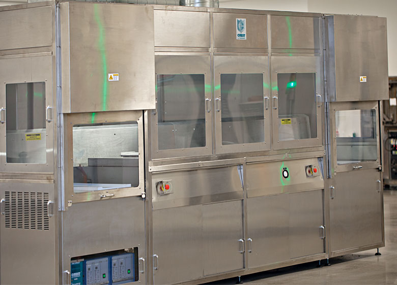
Click to Enlarge
Fully Automated Optical Cleaning System

Click to Enlarge
Optics After Cleaning
E-Beam Deposition
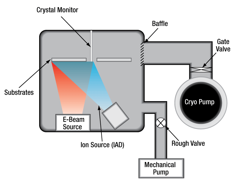
Thorlabs' coating facility currently operates four fully automated Electron Beam (E-Beam) deposition systems. These systems use an electron beam source to evaporate a selection of materials such as transition metal oxides (e.g., TiO2, Ta2O5, HfO2, Nb2O5, ZrO2), metal halides (MgF2, YF3), or SiO2. This type of process must be done at elevated temperatures (200 - 250 °C) to achieve good adhesion to the substrate and acceptable material properties in the final coating.
Ion-Assisted E-Beam Deposition
Ion-Beam Assisted Deposition (IAD) uses the same E-beam method to evaporate coating materials but with the addition of an ion source to promote nucleation and growth of materials at lower temperatures (20 - 100 °C). The ion source allows temperature-sensitive substrates to be coated. This process also results in a denser coating that is less sensitive to spectral shifting in both humid and dry environmental conditions.
IBS Deposition
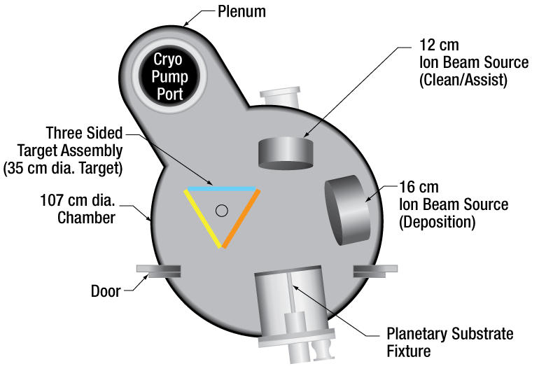
Our Ion Beam Sputtering (IBS) deposition chamber is the most recent addition to our line-up of coating tools. This process uses a high energy, radio frequency, plasma source to sputter coating materials and deposit them on substrates while another RF ion source (Assist source) provides IAD function during deposition. The sputtering mechanism can be characterized as momentum transfer between ionized gas molecules from the ion source and the atoms of the target material. This is analogous to a cue ball breaking a rack of billiard balls, only on a molecular scale and with several more balls in play.
Advantages of IBS
- Better Process Control
- Wider Selection of Coating Designs
- Improved Surface Quality and Less Scatter
- Reduced Spectral Shifting
- Thicker Coating in a Single Cycle
Click to Enlarge
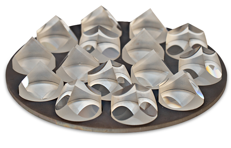
Coated Retroreflectors in Tool
Metrology
Thorlabs uses a selection of research-grade spectroscopy instruments to characterize coating performance from the UV to the Far Infrared. In addition to spectroscopy tools, we employ a variety of laser and laser diode sources, power meters, detectors, and polarimeters to test the performance of our optics. Specific metrology systems include Cary 660 FTIR, Cary 5000, PE Lambda 950, and Olis PE 983 IR spectrophotometers, a KLA Tencor surface profilometer, a J.A. Woollam RC2 ellipsometer, Zygo monochromatic interferometers, an Optoflat broadband interferometer for single surface and multi-surface interferometric measurements, a surface scatter instrument, and a custom-built cavity ring down system. All of these tools help us understand our coatings and materials at a molecular level. We build custom setups to test both catalog and OEM parts to ensure every optic we offer performs within the specified range. All metrology instruments are calibrated regularly per the ISO 9001:2015 standard.
Laser Line/Bandpass Filters
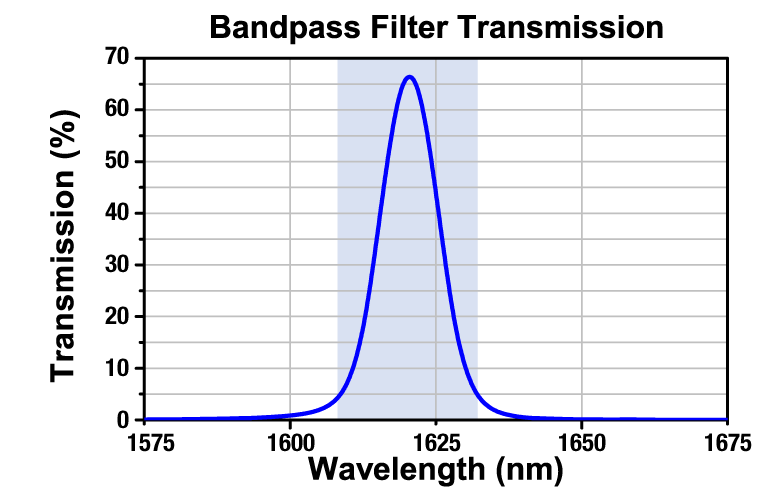
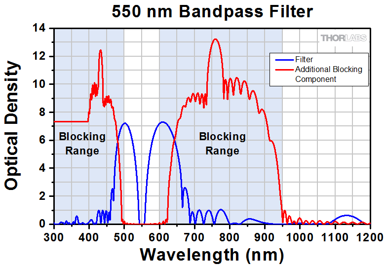
Laser Line and Bandpass filters transmit light in a narrow, well-defined spectral region while rejecting other unwanted radiation. This type of filter displays very high transmission in the bandpass region and blocks a limited spectral range of light on either side of the bandpass region. To compensate for this deficiency, an additional blocking component is added, which is either an all-dielectric or a metal-dielectric depending on the requirements of the filter. Although this additional blocking component eliminates any unwanted out-of-band radiation, it also reduces the filter's overall transmission throughput.
These coatings are formed by vacuum deposition coating techniques and consist of two reflecting stacks, separated by an even-order spacer layer. These reflecting stacks are constructed from alternating layers of high and low refractive index materials, which can have a reflectance in excess of 99.99%. By varying the thickness of the spacer layer and/or the number of reflecting layers, the central wavelength and bandwidth of the filter can be altered.
Edgepass Filters

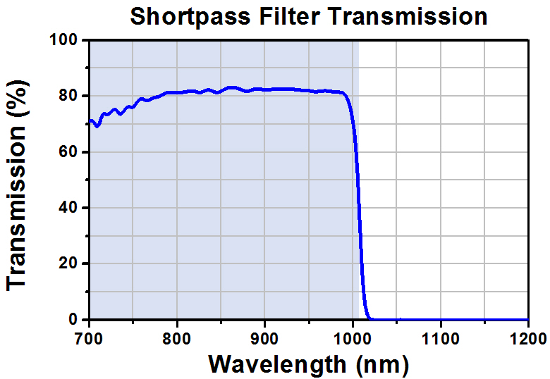
Edgepass filters are very useful for isolating specific spectral regions. Longpass filters transmit wavelengths longer than the cutoff wavelenght and block wavelengths shorter than the cutoff wavelength. Shortpass filters block wavelengths longer than the cutoff wavelength and transmit those shorter than the cutoff wavelength.
All Thorlabs edgepass filters are constructed of durable dielectric coatings and will withstand the normal cleaning and handling associated with any high-quality optical component. Their film construction is essentially a modified quarter-wave stack, using interference effects rather than absorption to isolate their spectral bands.
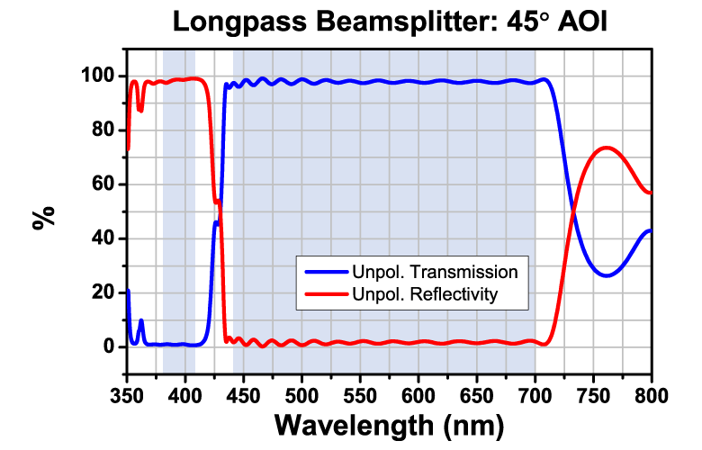
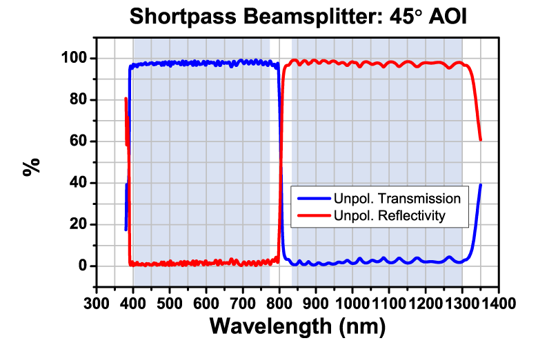
Dichroic Beamsplitters
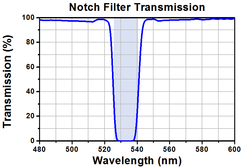
Notch Filters
 Click to Enlarge
Notch filters, also commonly referred to as band-stop or band-rejection filters, are designed to transmit most wavelengths but attenuate light within a specific wavelength range (the stop band) to a very low level. They are functionally the inverse of bandpass filters and are made in the same way.
Neutral Density Filters
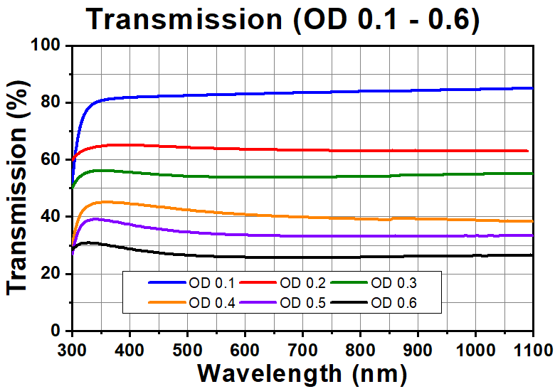
Neutral Density (ND) filters attenuate all wavelengths within a range by a certain factor to prevent damage to detecting equipment. Fixed ND filters attenuate the spectra by a fixed amount. Variable ND filters have stepped films at discrete locations to allow for various attenuation depending on the application. Continuous ND filters have a film gradient across the entire filter, which allows for a continuous range of attenuation. Thorlabs offers a selection of both linear and circular variable and continuous ND filters.

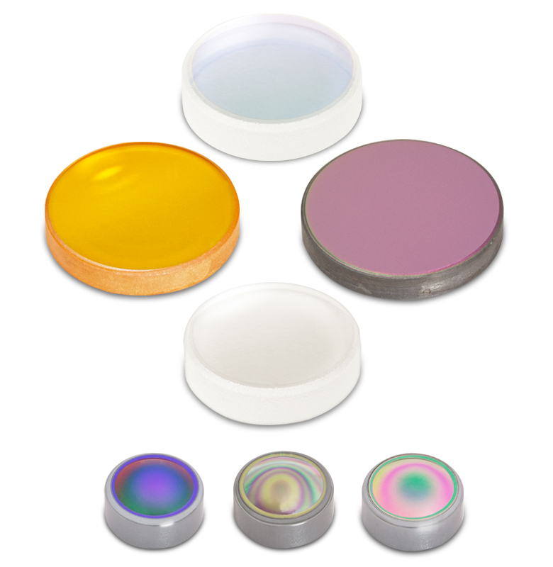
Antireflective (AR) Coatings
AR coatings are hard refractory-oxide coatings that minimize surface reflections within specified wavelength ranges when applied to the surface of optical components. Without AR coating, 4% of the light is lost at each optical surface due to reflections. For example, if three uncoated lenses are being used in series, this 4% loss occurs at each of the six optical surfaces. This results in a total loss of 21.7%. If three AR-coated lenses with a "B" coating (Ravg <0.5% per surface) are used instead, the total loss of incident light due to surface reflections is <3%. The use of AR-coated optics improves transmission from 78.3% to greater than 97% in this case. Please note that the 4% loss at the interfaces of uncoated optics is an approximate value that varies greatly with material and angle of incidence (AOI). Please note that the color of the lens does not correlate to the lens’ specifications. The color of each AR coating may vary from batch to batch and is not an indicator of performance.
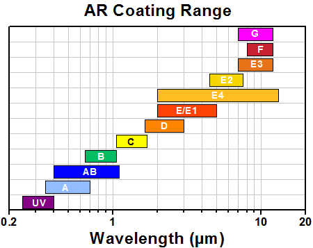
The AR Coating Range graph below shows the specified wavelength range of Thorlabs' in-house AR coatings. Click on the bars in the graph below to view the performance plot for each coating.
Broadband antireflective (BBAR) coatings consist of multiple layers, alternating between a high index material and a low index material. The layers are deposited on the substrate via electron-beam deposition. The thickness of the layers is optimized, using modeling software, to produce destructive interference between reflected waves and constructive interference between transmitted waves. This results in an optic that has enhanced performance within a specified wavelength band as well as minimal internal reflections (ghosting). Thorlabs' BBAR coatings provide good performance for angles of incidence between 0° and 30° and a numerical aperture (NA) of 0.5. Thorlabs currently offers BBAR coatings designed to maximize performance within 8 different wavelength ranges.
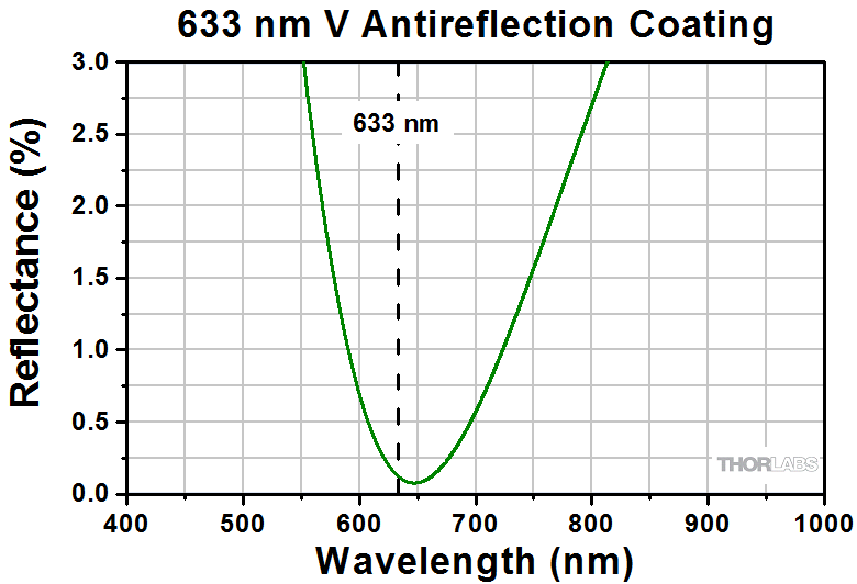
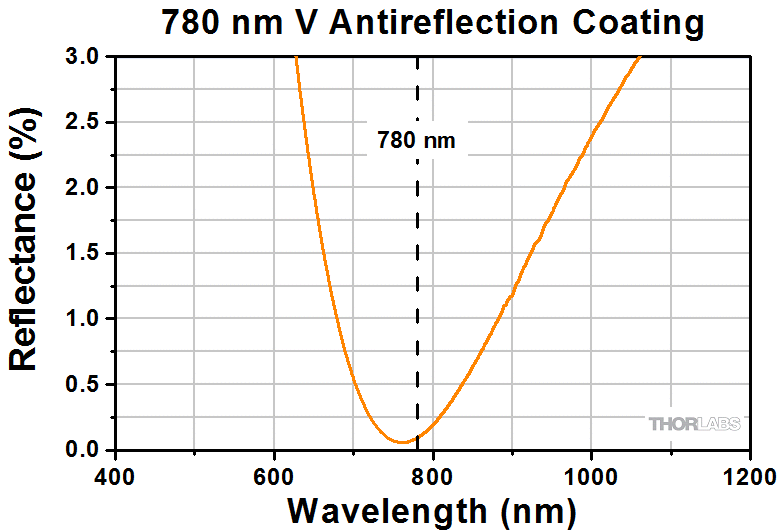
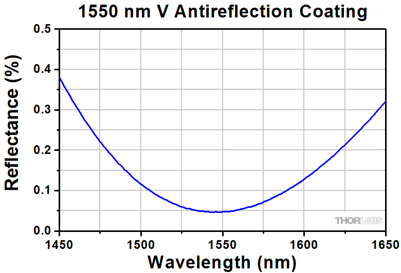
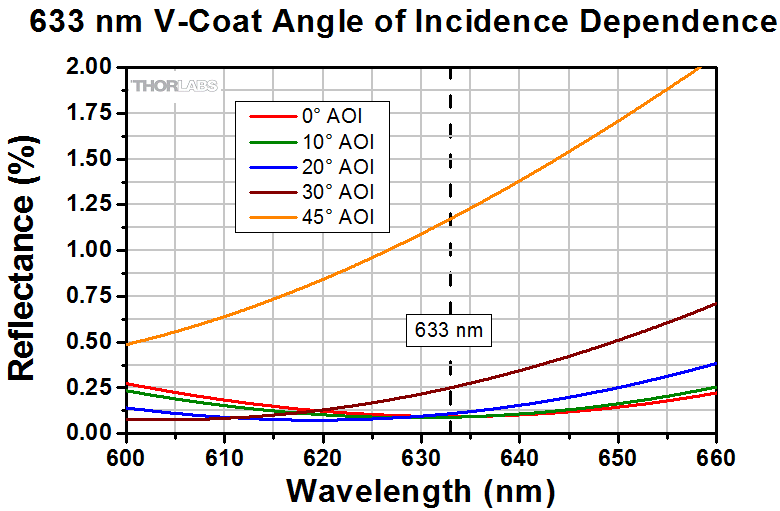
V-coatings are multilayer, dielectric, thin-film, AR coatings that are designed to minimize reflectance over a short wavelength range. Surface reflectance rises rapidly on either side of this minimum, which gives the reflectance curve a "V" shape. Compared to the broadband AR coatings, V-coatings achieve lower reflectance over a narrower bandwidth when used within their design AOI range. See the graph to the right for an example of the reflectance of a 633 nm V-coat designed for 0° AOI at various angles. We offer a variety of different V-coatings; see the table below for more information.
The tables below give the specifications for Thorlabs' in-house antireflection coatings, which are deposited on the surfaces of many optics and fibers in our catalog. However, we also offer optics that are coated by external vendors. As such, the specifications for some of our antireflection coated optics may be slightly different than the specifications given on this page. The AR coating specifications for any individual item are always included in that item's web presentation.
| Broadband Antireflective Coating Specifications | ||||
|---|---|---|---|---|
| Coating Code | Wavelength Range | Reflectancea | Performance Plotb |
Coating Variationc |
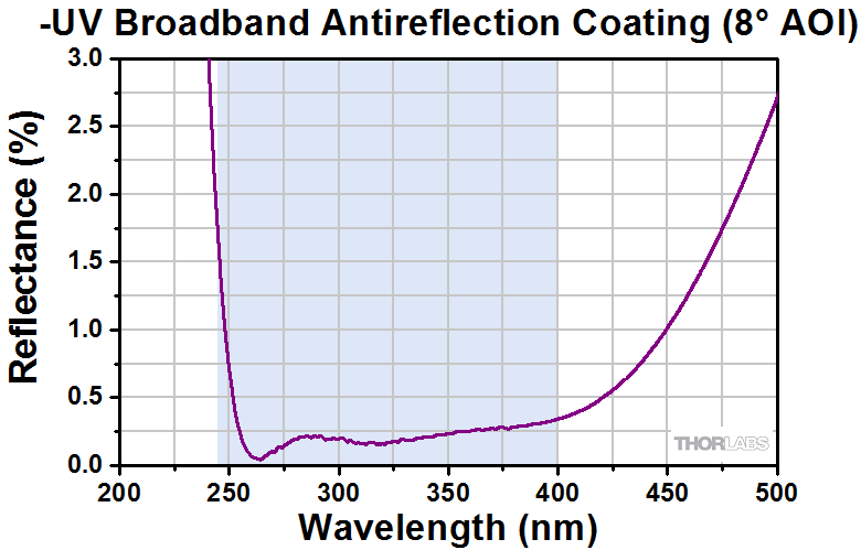
| UV | 245 - 400 nm | Ravg < 0.5% | Unavailable | |
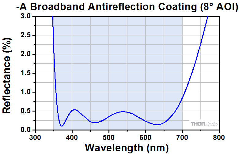
| A | 350 - 700 nm | Ravg < 0.5% | 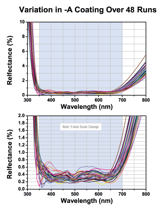 Raw Data |
|
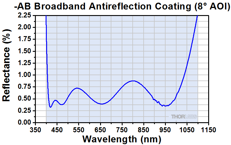
| AB | 400 - 1100 nm | Ravg < 1.0% | Unavailable | |
| B | 650 - 1050 nm | Ravg < 0.5% |  Raw Data |
|
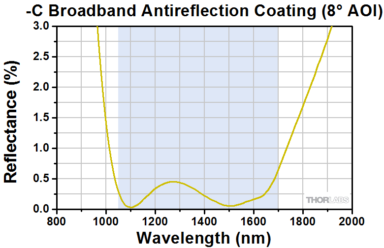
| C | 1050 - 1700 nmd | Ravg < 0.5% |  Raw Data |
|
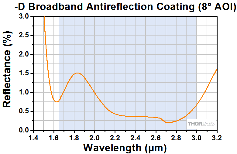
| D | 1.65 - 3.0 µm | Ravg < 1.0% | Unavailable | |
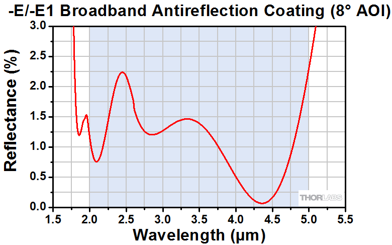
| Ee,f | 2 - 5 µm | Ravg < 1.25% | Unavailable | |
| E1f | 2 - 5 µm | Ravg < 1.50% Rabs < 3.0% |
||
| E4 | 2 - 13 µm | Ravg < 3.5% Rabs < 6% |
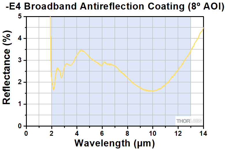 Raw Data |
Unavailable |
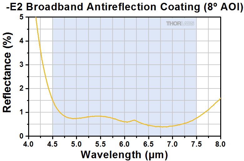
| E2 | 4.5 - 7.5 µm | Ravg < 1.0% Rabs < 2.0% |
Unavailable
|
|
| E3g | 7 - 12 µm | Ravg < 1.0% Rabs < 2.0% |
Unavailable | |
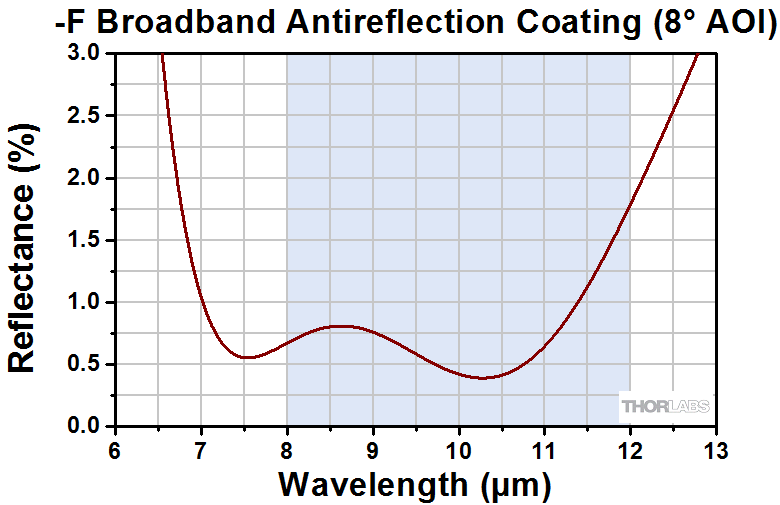
| F | 8 - 12 µm | Ravg < 1.5% | Unavailable | |
| Gg | 7 - 12 µm | Ravg < 1.0% | Unavailable | |

| Narrowband Antireflective (V-) Coating Specifications | |||
|---|---|---|---|
| Coating Code | Design Wavelength | Reflectance per Surfacea |
Performance Plot |
| 405 | 405 nm | <0.25% |  Raw Data |
| 532 | 532 nm | <0.25% | 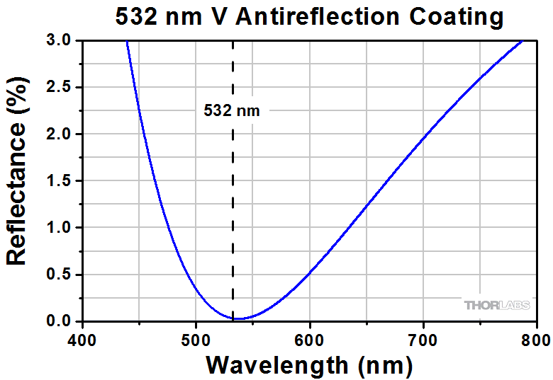 Raw Data |
| 633 | 633 nm | <0.25% | |
| 780 | 780 nm | <0.25% | |
| 1064 | 1064 nm | <0.25% | 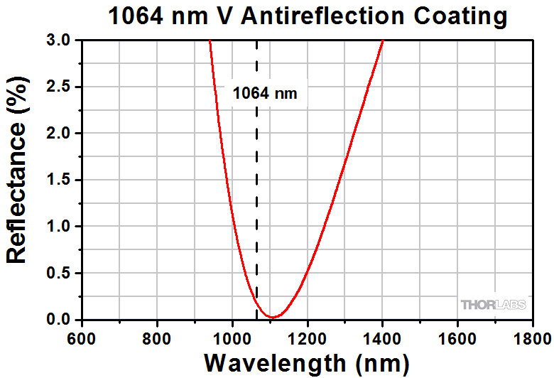 Raw Data |
| YAG | 532/1064 nm | <0.25% | |
| 1550 | 1550 nm | <0.25% | |

Click to Enlarge
Dependence of Reflectance on Angle of Incidence
for a 633 nm V-Coat Designed for 0° AOI
 Thorlabs' Selection of HR-Coated Optics
Table of Contents
Thorlabs offers dielectric and metallic broadband coatings, dielectric narrowband coatings for laser line applications, and high-performance crystalline mirror coatings. We also offer a selection of ultrafast mirrors optimized for femtosecond laser pulse applications.
Thorlabs' dielectric HR coatings, available in broadband and narrowband designs, are hard, refractory, oxide coatings that maximize surface reflections within specified wavelength ranges and at specified angles of incidence. These coatings consist of alternating layers of high- and low-index materials. Using computer models, the thickness of each layer is optimized to produce constructive interference for reflected waves and destructive interference for transmitted waves.
The reflectance of surfaces can be greatly improved by the addition of an HR coating; however, performance will depend on both the wavelength and the angle of incidence (AOI). At high AOIs, the performance will also depend on the polarization of the incident light. Information about the reflectance of each HR coating can be found in the tables below.
Broadband HR Coatings
Thorlabs offers a number of broadband HR coatings optimized for various performance parameters. The graph below shows the specified wavelength range of Thorlabs' in-house broadband HR coatings. Click on the bars in the graph below to view the performance plot for each coating. Click here for a raw data file that compares all of our broadband HR Coatings.
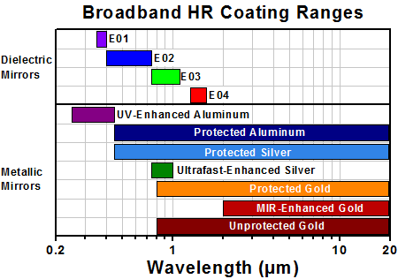
The E01, E02, E03, and E04 dielectric HR coatings offer high reflectance over broad wavelength ranges. Our UV-Enhanced Aluminum coating has an overcoat of MgF2 to increase its average reflectance in the UV portion of the spectrum. The Protected Aluminum coating is an inexpensive solution and has an overcoat of SiO2 to make the aluminum coating suitable for laboratory and industrial use. The Protected Silver coating has the highest reflectance in the visible spectrum and is protected with an SiO2 overcoat to prevent oxidation. The Ultrafast-Enhanced Silver coating is manufactured such that it exhibits a low group delay dispersion. Three gold coating options are offered: protected, MIR enhanced, and unprotected. The Protected Gold coating retains a high reflectance down to 800 nm, while the MIR enhanced gold coating is optimized to reduce losses in the MIR that are commonly found in gold mirrors. Each of these gold coatings is protected by an overcoat that also makes the mirrors easy to clean. The Unprotected Gold coating offers higher reflectance than the protected gold coating, but is slightly more delicate.
| Broadband HR Coating Specifications | ||||||||
|---|---|---|---|---|---|---|---|---|
| Coating Namea | Wavelength Range |
Avg. Reflectanceb | Angle of Incidence | Graphs | Pulsed Laser Damage Threshold for UV Fused Silicac |
CW Laser Damage Threshold for UV Fused Silicad |
||
| E01 | 350 - 400 nm | >99% | 0° to 45° | 1 J/cm2 (355 nm, 10 ns, 10 Hz, Ø0.373 mm) | - | |||
| E02 | 400 - 750 nm | >99% | 0° to 45° |
|
0.25 J/cm2 (532 nm, 10 ns, 10 Hz, Ø0.803 mm) | 550 W/cm (532 nm, Ø1.000 mm) | ||
| E03 | 750 - 1100 nm | >99% | 0° to 45° | 0.205 J/cm2 (800 nm, 99 fs, 1 kHz, Ø0.166 mm) 1 J/cm2 (810 nm, 10 ns, 10 Hz, Ø0.133 mm) 0.5 J/cm2 (1064 nm, 10 ns, 10 Hz, Ø0.433 mm) |
10 kW/cm (1070 nm, Ø0.971 mm) | |||
| E04 | 1280 - 1600 nm | >99% | 0° to 45° | 2.5 J/cm2 (1542 nm, 10 ns, 10 Hz, Ø0.181 mm) | 350 W/cm (1540 nm, Ø1.030 mm) | |||
| UV-Enhanced Aluminum (-F01) |
250 - 450 nm | >90% | 0° to 45° | 0.25 J/cm2 (266 nm, 10 ns, 10 Hz, Ø0.150 mm) 0.3 J/cm2 (355 nm, 10 ns, 10 Hz, Ø0.381 mm) |
300 W/cm (1.064 µm, Ø0.044 mm) 500 W/cm (10.6 µm, Ø0.339 mm) |
|||
| Protected Aluminum (-G01) |
450 nm - 20 µm | >90% (450 nm - 2 µm) >95% (2 - 20 µm) |
0° to 45° | 0.3 J/cm2 (1064 nm, 10 ns, 10 Hz, Ø1.000 mm) | 100 W/cm (1.070 µm, Ø0.098 mm) 350 W/cm (10.6 µm, Ø0.339 mm) |
|||
| Ultrafast-Enhanced Silver (-AG) |
750 nm - 1 µm | Rabsolute,S > 99.0% Rabsolute,P > 98.5% |
45° | 0.18 J/cm2 (800 nm, 52 fs FWHM S-Pol, 1000 Pulses)e 0.39 J/cm2 (800 nm, 52 fs FWHM S-Pol, Single Pulse)e |
- | |||
| Protected Silver (-P01) | 450 nm - 20 µm | >96.5% (450 nm - 2 µm)f,g >95% (2 - 20 µm) |
0° to 45° | 0.225 J/cm2 (800 nm, 99 fs, 1 kHz, Ø0.167 mm) 1 J/cm2 (1064 nm, 10 ns, 10 Hz, Ø1.010 mm) |
500 W/cm (1.07 µm, Ø0.974 mm) 1500 W/cm (10.6 µm, Ø0.339 mm) |
|||
| Protected Silver (-P02)h | 450 nm - 20 µm | >97% (450 nm - 2 µm) >95% (2 - 20 µm) |
0° to 45° | - | - | |||
| Protected Gold (-M01) | 800 nm - 20 µm | >96% | 0° to 45° | 2 J/cm2 (1064 nm, 10 ns, 10 Hz, Ø1.000 mm) | 500 W/cm (1.070 µm, Ø0.089 mm) 750 W/cm (10.6 µm, Ø0.339 mm) |
|||
| MIR Enhanced Gold (-M02) |
2 - 20 µm | >98% | 0° to 45° | 0.1 J/cm2 (1.064 µm, 10 ns, 10 Hz, Ø1.06 mm) 3 J/cm2 (10.6 µm, 100 ns, 1 Hz, Ø1.29 mm) |
25 W/cm (1.07 µm, Ø1.04 mm) 450 W/cm (10.6 µm, Ø1.18 mm) |
|||
| Unprotected Gold (-M03) | 800 nm - 20 µm | >97% | 0° to 45° | 4 J/cm2 (10.6 µm, 100 ns, 1 Hz, Ø0.435 mm) | 1000 W/cm (10.6 µm, Ø1.18 mm) | |||
Narrowband Laser Line HR Coatings
Thorlabs offers a number of laser line HR coatings optimized for various performance parameters. These dielectric HR coatings offer very high reflectance over specific laser line wavelength ranges.
| Narrowband Laser Line HR Coating Specifications | |||||||
|---|---|---|---|---|---|---|---|
| Coating Namea | Wavelength Range |
Laser Line | Average Reflectanceb | Angle of Incidence |
Graphs | Pulsed Laser Damage Thresholdc | CW Laser Damage Thresholdd |
| K04 | 262 - 266 nm | Nd:YAG, 4th Harmonic |
>99.0% (S- and P-Pol) | 0° to 45° | 2 J/cm2 (266 nm, 10 ns, 10 Hz, Ø0.416 mm) | - | |
| K05 | 300 - 308 nm | Ar Ion | >99.5% (S-Pol) >98.0% (P-Pol) |
0° to 45° | - | - | |
| K07 | 333 - 364 nm | Ar Ion | >99.5% (S-Pol, 45° AOI)e >99.0% (P-Pol, 45° AOI)e >98.7% (Unpol, 0° AOI)e |
0° to 45° | 5 J/cm2 (355 nm, 10 ns, 10 Hz, Ø0.294 mm) | - | |
| K08 | 349 - 355 nm | Nd:YAG, 3rd Harmonic |
>99.5% (S- and P-Pol) | 0° to 45° | 3.5 J/cm2 (355 nm, 10 ns, 10 Hz, Ø0.350 mm) | - | |
| K10 | 458 - 528 nm | Ar Ion | >99.0% (S- and P-Pol) | 0° to 45° | - | - | |
| J11 | 520 - 647 nm | Kr Ion | >99.7% (S- and P-Pol) | 45° | - | - | |
| K12 | 524 - 532 nm | Nd:YAG, 2nd Harmonic |
>99.5% (S-Pol) >99.0% (P-Pol) |
0° to 45° | 8 J/cm2 (532 nm, 10 ns, 10 Hz, Ø0.491 mm) | 550 W/cm (532 nm, Ø1.000 mm) | |
| K13f (Dual Coating) |
532 nm | Nd:YAG, 2nd Harmonic |
>98.0% (S- and P-Pol) | 0° to 45° | 8 J/cm2 (532 nm, 10 ns, 10 Hz, Ø0.491 mm) | - | |
| 1064 nm | Nd:YAG | >99.0% (S- and P-Pol) | 0° to 45° | 5 J/cm2 (1064 nm, 10 ns, 10 Hz, Ø1.010 mm) | |||
| K14 | 1047 - 1064 nm | Nd:YAG | >99.5% (S- and P-Pol) | 0° to 45° | 25 J/cm2 (1064 nm, 10 ns, 10 Hz, Ø0.552 mm) | 20 kW/cm (1070 nm, Ø0.974 mm) | |
| L01 | 10.6 µm | CO2 | >99% (S- and P-Pol) | 0° to 45° | 6 J/cm2 (10.6 µm, 100 ns, 1 Hz, Ø0.362 mm) | 10 kW/cm (Ø0.115 mm) | |
Crystalline Mirror Coatings
Thorlabs Crystalline Solutions currently offers three different GaAs/AlGaAs crystalline coatings optimized for superior mid-IR performance, as well as the ability to create custom crystalline coatings. These high-reflectance mirror coatings are ideal for high-finesse laser cavities, precision interferometry, and high-power laser systems. The specifications below are typical values. Thorlabs offers a selection of concave and plano xtal stable™-coated mirrors from stock. Mirrors with xtal mir™ or xtal therm™ coatings, as well as custom mirrors with xtal stable™ coatings, are made to order by request through Tech Support.
| Crystalline HR Coating Specifications | ||||||||
|---|---|---|---|---|---|---|---|---|
| Coating Namea | Center Wavelengths From Stock |
Custom Center Wavelengths Available Betweenb |
Reflectancec | Loss Angled | Pulsed Laser Damage Thresholde | CW Laser Damage Thresholdf | ||
| xtal stable™ | 1064 nm, 1156 nm, 1397 nm, and 1550 nm |
900 nm and 2.0 µm | >99.99% (Typical) >99.999% (Max) |
<4 x 10⁻⁵ at 300 K <5 x 10⁻⁶ at 10 K |
5 J/cm2 (1030 nm, 10 ns, 10 Hz, Ø0.240 mm) | 46.2 kW/cm (1064 nm, Ø5.5 mm) | ||
| xtal mir™ | - | 2.0 µm and 5.0 µm | ||||||
| xtal therm™ | - | 900 nm and 5.0 µm | ||||||
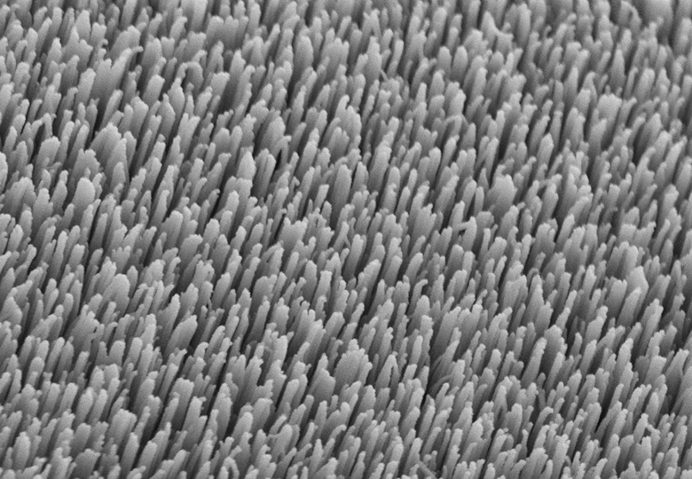
Click to Enlarge
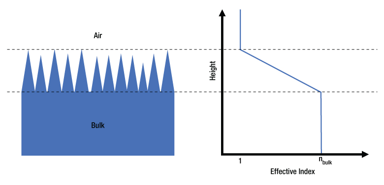
The conical nanostructures making up our textured surfaces produce a continuous gradient in the effective index from air to the bulk material.
Click to Enlarge
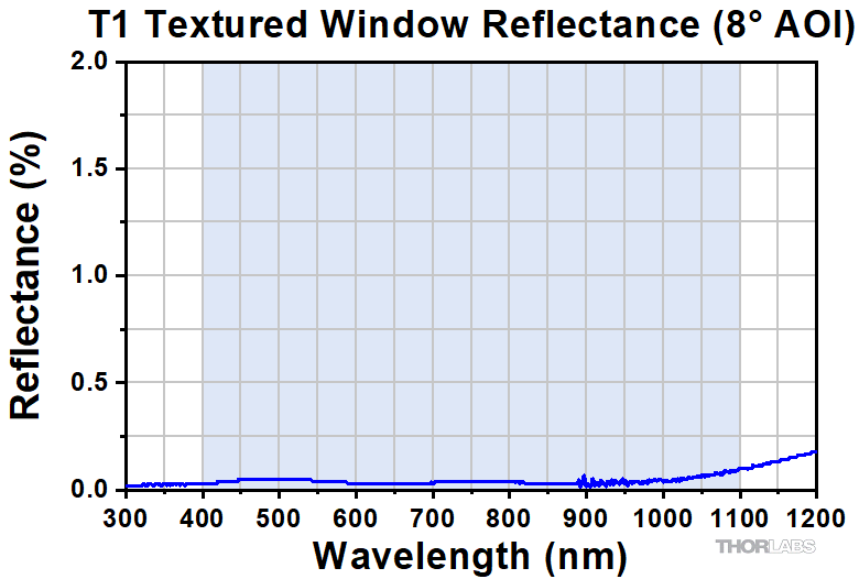
An SEM image showing a top-view of the T1 textured AR surface.
Textured AR Surfaces
Thorlabs' textured AR surfaces are created by removing material from the bulk optic substrate using our proprietary process, which has been optimized to fabricate subwavelength structures. The surface that remains consists of roughly conical nanostructures, with irregular spacing and varied height. These nanostructures produce a smooth gradient of the effective refractive index.
Since there are no step changes in the refractive index, the incident light is able to travel from the air to the bulk glass with virtually no Fresnel reflections. As a result, textured optics can achieve significantly higher transmission than un-textured optics. Thorlabs currently offers three surfaces for stock optics (see the table below for details).
Antireflection Performance
Compared to our traditional thin-film broadband antireflective (BBAR) coatings, our textured surfaces exhibit lower reflectance over a broad wavelength range and lower angular sensitivity. The anti-reflection mechanism used in dielectric AR coatings is based on the interference between reflections from subsequent thin film dielectric layers. This behavior is highly dependent on the wavelength of the light, as the refractive indices and thicknesses of each layer are designed to provide the desired phase relationship between reflecting waves. Moreover, the angle of incidence (AOI) affects the effective thickness of each layer that the light interacts with, which leads to a strong dependence on the AOI. As a result, there are limitations on the performance that a BBAR coating can achieve over a broad range of wavelengths and AOIs.
In contrast, the effective index gradient of our textured surfaces is less sensitive to the wavelength and AOI than thin-film interference, allowing for very low reflectance over a broad range of both. See the graphs below for an illustration of this difference.
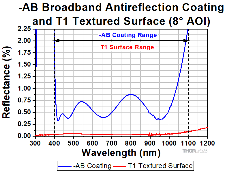 Click to Enlarge
 Comparison of Thorlabs' -AB thin-film BBAR coating and the T1 textured surface reflectances. While both have a 400 - 1100 nm wavelength range, the T1 surface has much lower reflectance.
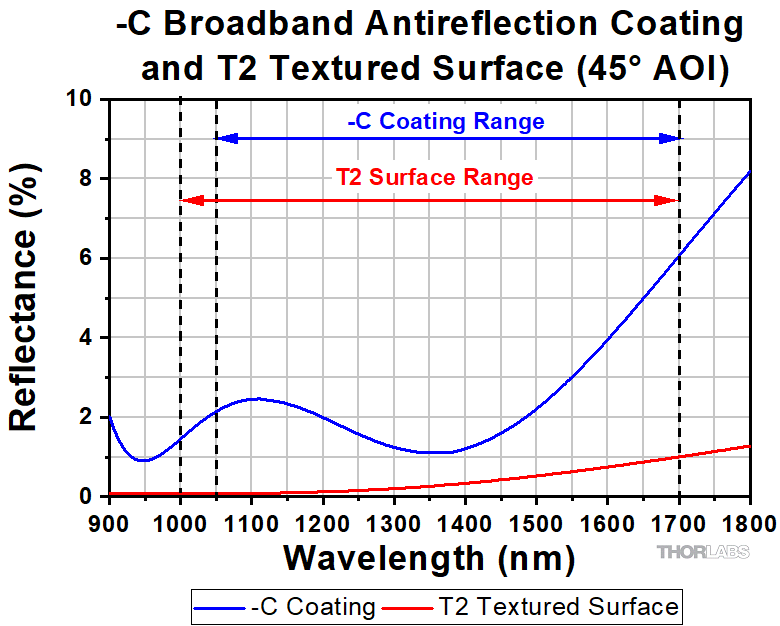 Click to Enlarge
 Comparison of Thorlabs' -C thin-film BBAR coating and the T2 textured surface reflectances for unpolarized light at 45° AOI. The T2 surface maintains much lower reflectance at high AOIs.
Click to Enlarge
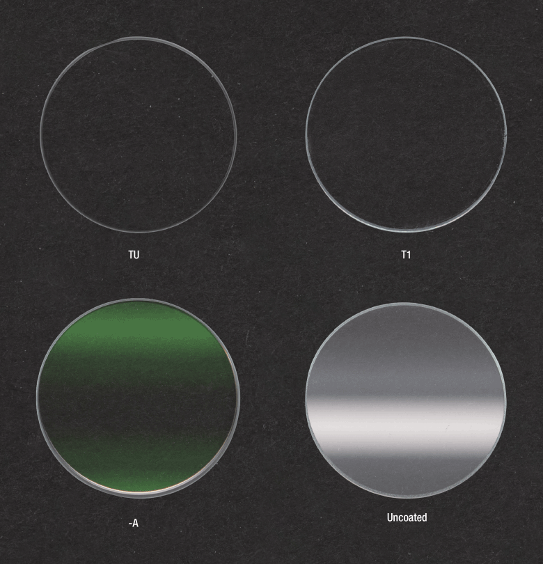
The superior antireflective performance of our textured surfaces can be observed by eye. In this image, four 1.0 mm thick UVFS windows were exposed to fluorescent ceiling lights, and reflections from the surfaces of the uncoated and A-coated windows can be seen in this photo. The windows with TU and T1 surfaces show no visible reflections.
Damage Threshold and Durability
Because the nanostructures comprising Thorlabs' textured surfaces are originally part of the bulk optic, they have substantially higher laser-induced damage thresholds than BBAR coatings. Laser-induced damage at moderate fluence typically originates from the interface between two materials, and the large number of thin-film layers in BBAR coatings increase the likelihood of damage. As our textured surfaces consist of the same material as the bulk, the damage threshold is higher.
When properly handled, textured surfaces can exhibit greater durability than BBAR coatings. Their single-material construction means that they do not suffer from mismatched coefficients of thermal expansion (CTE) under temperature cycling and avoid issues with thin-film adhesion that can occur in some AR coatings.
| Textured AR Surface Specifications | |||
|---|---|---|---|
| Surface Name | TU | T1 | T2 |
| Substrate | UV Fused Silica | Infrasil ®† | |
| Wavelength Range | 230 - 450 nm | 400 - 1100 nm | 1000 - 1700 nm |
| Damage Threshold | >30 J/cm 2 at 355 nm, 10 ns, 10 Hz, Ø0.22 mm |
>30 J/cm 2 at 532 nm, 10 ns, 10 Hz, Ø0.4 mm |
>30 J/cm 2 at 1064 nm, 10 ns, 10 Hz, Ø0.23 mm |
| Reflectance Over Wavelength Range a |
R avg < 0.25% | ||
| Reflectance Data (Click for Graph) |
 Raw Data |
 Raw Data |
 Raw Data |
Handling Precautions and Cleaning
Thorlabs' Textured Windows could be contaminated or damaged by moisture, fingerprints, aerosols, or contact with any abrasive material. The windows should only be handled when necessary and always held by the sides using our TZ2 or TZ3 tweezers. Latex gloves or a similar protective covering should be worn to prevent oil from fingers from reaching the structured surface.
If the surface is contaminated, the windows may be cleaned by:
- Blowing off dust with clean air or nitrogen.
- Rinsing with solvents, such as isopropyl alcohol, followed by clean air or nitrogen blow-drying.
- Immersing in a basic solution (a mix of ammonium hydroxide and hydrogen peroxide) and/or an acid solution (a mix of hydrogen chloride and hydrogen peroxide) followed by clean air or nitrogen blow-drying.
Standard cleaning methods will result in further contamination and thus should be avoided.
†Infrasil is a registered trademark of Heraeus Quarzglas.
Absolute and Average Reflectance
Thorlabs quotes two types of reflectance values for our optical coatings. Absolute Reflectance (Rabs, or simply R) indicates the maximum or minimum reflectance at a specific wavelength or wavelengths. When specified over a wavelength range, it indicates the maximum or minimum reflectance for each wavelength within the range. The reflectance may increase or decrease sharply near the specified wavelengths or wavelength range, as in our V-coatings.
The other type of reflectance specification is Average Reflectance (Ravg), which is always quoted over a wavelength range. Ravg is found by measuring the reflectance at wavelengths across the specified range and then averaging the reflectance over wavelength. This specification is insensitive to certain variations between individual coating runs that may not be of interest for broadband applications. If a guarantee of performance at a particular wavelength is needed, then a coating specified by Rabs will be preferable.
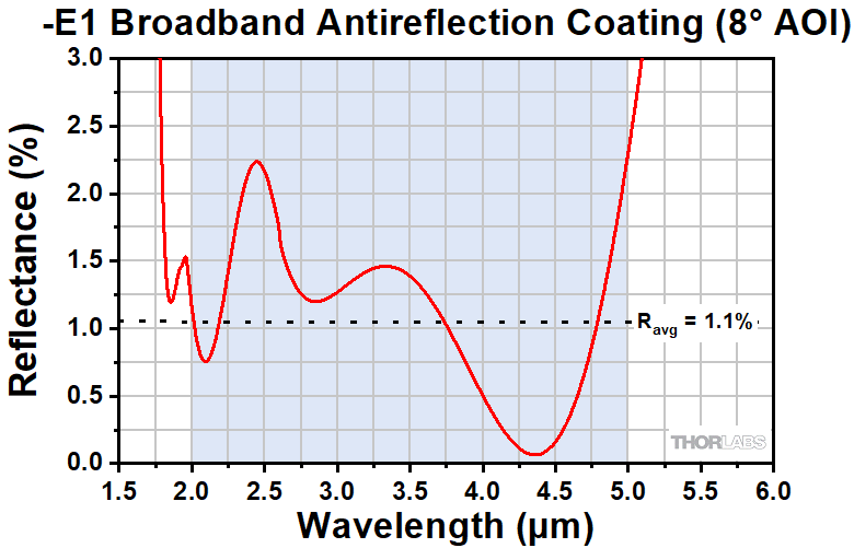
Click to Enlarge
Thorlabs' -E1 broadband antireflective coating is specified to have Ravg < 1.5% and Rabs < 3% over the 2 - 5 μm range. The reflectance (Rabs) for the representative coating shown here exceeds 1.5% at some wavelengths within that range, but never exceeds 3%.
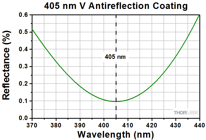
Click to Enlarge
Thorlabs' 405 nm V-coating is specified to have Rabs < 0.25% at 405 nm. The reflectance (Rabs) can be seen to increase rapidly away from 405 nm.
Run-to-Run Variation
The plot below shows reflectance data from four -P01 coatings produced by Thorlabs. While all four meet the average reflectance specification from 450 - 2000 nm, their reflectances differ at specific wavelengths. The variation is largest below 850 nm, where all four coatings have reflectances lower than 96.5%. This kind of behavior is typical of coatings specified by Ravg. Outside of the specified range, the variation can be more pronounced, because the reflectance at those wavelengths is not controlled.
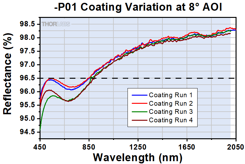
Click to Enlarge
8° AOI reflectance curves for four representative -P01 coating runs. The coating
is specified to have Ravg > 96.5% (dashed line) over the 450 - 2000 nm range (blue-shaded region). While all four coatings meet that specification, they all have absolute reflectances less than 96.5% for wavelengths below 850 nm. The individual coating runs also differ in their absolute reflectances at each wavelength.
Laser Induced Damage Threshold Tutorial
The following is a general overview of how laser induced damage thresholds are measured and how the values may be utilized in determining the appropriateness of an optic for a given application. When choosing optics, it is important to understand the Laser Induced Damage Threshold (LIDT) of the optics being used. The LIDT for an optic greatly depends on the type of laser you are using. Continuous wave (CW) lasers typically cause damage from thermal effects (absorption either in the coating or in the substrate). Pulsed lasers, on the other hand, often strip electrons from the lattice structure of an optic before causing thermal damage. Note that the guideline presented here assumes room temperature operation and optics in new condition (i.e., within scratch-dig spec, surface free of contamination, etc.). Because dust or other particles on the surface of an optic can cause damage at lower thresholds, we recommend keeping surfaces clean and free of debris. For more information on cleaning optics, please see our Optics Cleaning tutorial.
Testing Method
Thorlabs' LIDT testing is done in compliance with ISO/DIS 11254 and ISO 21254 specifications.
First, a low-power/energy beam is directed to the optic under test. The optic is exposed in 10 locations to this laser beam for 30 seconds (CW) or for a number of pulses (pulse repetition frequency specified). After exposure, the optic is examined by a microscope (~100X magnification) for any visible damage. The number of locations that are damaged at a particular power/energy level is recorded. Next, the power/energy is either increased or decreased and the optic is exposed at 10 new locations. This process is repeated until damage is observed. The damage threshold is then assigned to be the highest power/energy that the optic can withstand without causing damage. A histogram such as that below represents the testing of one BB1-E02 mirror.
The photograph above is a protected aluminum-coated mirror after LIDT testing. In this particular test, it handled 0.43 J/cm2 (1064 nm, 10 ns pulse, 10 Hz, Ø1.000 mm) before damage.
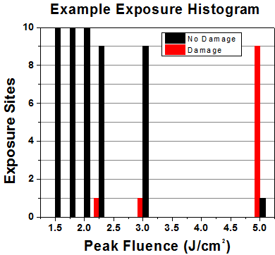
| Example Test Data | |||
|---|---|---|---|
| Fluence | # of Tested Locations | Locations with Damage | Locations Without Damage |
| 1.50 J/cm2 | 10 | 0 | 10 |
| 1.75 J/cm2 | 10 | 0 | 10 |
| 2.00 J/cm2 | 10 | 0 | 10 |
| 2.25 J/cm2 | 10 | 1 | 9 |
| 3.00 J/cm2 | 10 | 1 | 9 |
| 5.00 J/cm2 | 10 | 9 | 1 |
According to the test, the damage threshold of the mirror was 2.00 J/cm2 (532 nm, 10 ns pulse, 10 Hz, Ø0.803 mm). Please keep in mind that these tests are performed on clean optics, as dirt and contamination can significantly lower the damage threshold of a component. While the test results are only representative of one coating run, Thorlabs specifies damage threshold values that account for coating variances.
Continuous Wave and Long-Pulse Lasers
When an optic is damaged by a continuous wave (CW) laser, it is usually due to the melting of the surface as a result of absorbing the laser's energy or damage to the optical coating (antireflection) [1]. Pulsed lasers with pulse lengths longer than 1 µs can be treated as CW lasers for LIDT discussions.
When pulse lengths are between 1 ns and 1 µs, laser-induced damage can occur either because of absorption or a dielectric breakdown (therefore, a user must check both CW and pulsed LIDT). Absorption is either due to an intrinsic property of the optic or due to surface irregularities; thus LIDT values are only valid for optics meeting or exceeding the surface quality specifications given by a manufacturer. While many optics can handle high power CW lasers, cemented (e.g., achromatic doublets) or highly absorptive (e.g., ND filters) optics tend to have lower CW damage thresholds. These lower thresholds are due to absorption or scattering in the cement or metal coating.

LIDT in linear power density vs. pulse length and spot size. For long pulses to CW, linear power density becomes a constant with spot size. This graph was obtained from [1].
Pulsed lasers with high pulse repetition frequencies (PRF) may behave similarly to CW beams. Unfortunately, this is highly dependent on factors such as absorption and thermal diffusivity, so there is no reliable method for determining when a high PRF laser will damage an optic due to thermal effects. For beams with a high PRF both the average and peak powers must be compared to the equivalent CW power. Additionally, for highly transparent materials, there is little to no drop in the LIDT with increasing PRF.
In order to use the specified CW damage threshold of an optic, it is necessary to know the following:
- Wavelength of your laser
- Beam diameter of your beam (1/e2)
- Approximate intensity profile of your beam (e.g., Gaussian)
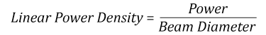
- Linear power density of your beam (total power divided by 1/e2 beam diameter)
Thorlabs expresses LIDT for CW lasers as a linear power density measured in W/cm. In this regime, the LIDT given as a linear power density can be applied to any beam diameter; one does not need to compute an adjusted LIDT to adjust for changes in spot size, as demonstrated by the graph to the right. Average linear power density can be calculated using the equation below.
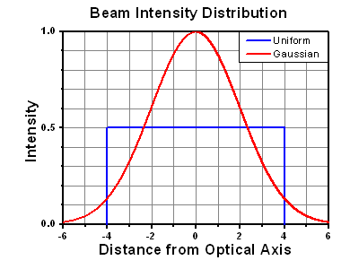
The calculation above assumes a uniform beam intensity profile. You must now consider hotspots in the beam or other non-uniform intensity profiles and roughly calculate a maximum power density. For reference, a Gaussian beam typically has a maximum power density that is twice that of the uniform beam (see lower right).
Now compare the maximum power density to that which is specified as the LIDT for the optic. If the optic was tested at a wavelength other than your operating wavelength, the damage threshold must be scaled appropriately. A good rule of thumb is that the damage threshold has a linear relationship with wavelength such that as you move to shorter wavelengths, the damage threshold decreases (i.e., a LIDT of 10 W/cm at 1310 nm scales to 5 W/cm at 655 nm):
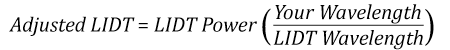
While this rule of thumb provides a general trend, it is not a quantitative analysis of LIDT vs wavelength. In CW applications, for instance, damage scales more strongly with absorption in the coating and substrate, which does not necessarily scale well with wavelength. While the above procedure provides a good rule of thumb for LIDT values, please contact Tech Support if your wavelength is different from the specified LIDT wavelength. If your power density is less than the adjusted LIDT of the optic, then the optic should work for your application.
Please note that we have a buffer built in between the specified damage thresholds online and the tests which we have done, which accommodates variation between batches. Upon request, we can provide individual test information and a testing certificate. The damage analysis will be carried out on a similar optic (customer's optic will not be damaged). Testing may result in additional costs or lead times. Contact Tech Support for more information.
Pulsed Lasers
As previously stated, pulsed lasers typically induce a different type of damage to the optic than CW lasers. Pulsed lasers often do not heat the optic enough to damage it; instead, pulsed lasers produce strong electric fields capable of inducing dielectric breakdown in the material. Unfortunately, it can be very difficult to compare the LIDT specification of an optic to your laser. There are multiple regimes in which a pulsed laser can damage an optic and this is based on the laser's pulse length. The highlighted columns in the table below outline the relevant pulse lengths for our specified LIDT values.
Pulses shorter than 10-9 s cannot be compared to our specified LIDT values with much reliability. In this ultra-short-pulse regime various mechanics, such as multiphoton-avalanche ionization, take over as the predominate damage mechanism [2]. In contrast, pulses between 10-7 s and 10-4 s may cause damage to an optic either because of dielectric breakdown or thermal effects. This means that both CW and pulsed damage thresholds must be compared to the laser beam to determine whether the optic is suitable for your application.
| Pulse Duration | t < 10-9 s | 10-9 < t < 10-7 s | 10-7 < t < 10-4 s | t > 10-4 s |
|---|---|---|---|---|
| Damage Mechanism | Avalanche Ionization | Dielectric Breakdown | Dielectric Breakdown or Thermal | Thermal |
| Relevant Damage Specification | No Comparison (See Above) | Pulsed | Pulsed and CW | CW |
When comparing an LIDT specified for a pulsed laser to your laser, it is essential to know the following:
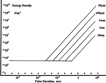
LIDT in energy density vs. pulse length and spot size. For short pulses, energy density becomes a constant with spot size. This graph was obtained from [1].
- Wavelength of your laser
- Energy density of your beam (total energy divided by 1/e2 area)
- Pulse length of your laser
- Pulse repetition frequency (prf) of your laser
- Beam diameter of your laser (1/e2 )
- Approximate intensity profile of your beam (e.g., Gaussian)
The energy density of your beam should be calculated in terms of J/cm2. The graph to the right shows why expressing the LIDT as an energy density provides the best metric for short pulse sources. In this regime, the LIDT given as an energy density can be applied to any beam diameter; one does not need to compute an adjusted LIDT to adjust for changes in spot size. This calculation assumes a uniform beam intensity profile. You must now adjust this energy density to account for hotspots or other nonuniform intensity profiles and roughly calculate a maximum energy density. For reference a Gaussian beam typically has a maximum energy density that is twice that of the 1/e2 beam.
Now compare the maximum energy density to that which is specified as the LIDT for the optic. If the optic was tested at a wavelength other than your operating wavelength, the damage threshold must be scaled appropriately [3]. A good rule of thumb is that the damage threshold has an inverse square root relationship with wavelength such that as you move to shorter wavelengths, the damage threshold decreases (i.e., a LIDT of 1 J/cm2 at 1064 nm scales to 0.7 J/cm2 at 532 nm):
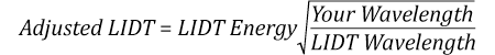
You now have a wavelength-adjusted energy density, which you will use in the following step.
Beam diameter is also important to know when comparing damage thresholds. While the LIDT, when expressed in units of J/cm², scales independently of spot size; large beam sizes are more likely to illuminate a larger number of defects which can lead to greater variances in the LIDT [4]. For data presented here, a <1 mm beam size was used to measure the LIDT. For beams sizes greater than 5 mm, the LIDT (J/cm2) will not scale independently of beam diameter due to the larger size beam exposing more defects.
The pulse length must now be compensated for. The longer the pulse duration, the more energy the optic can handle. For pulse widths between 1 - 100 ns, an approximation is as follows:
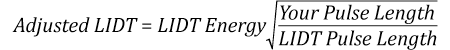
Use this formula to calculate the Adjusted LIDT for an optic based on your pulse length. If your maximum energy density is less than this adjusted LIDT maximum energy density, then the optic should be suitable for your application. Keep in mind that this calculation is only used for pulses between 10-9 s and 10-7 s. For pulses between 10-7 s and 10-4 s, the CW LIDT must also be checked before deeming the optic appropriate for your application.
Please note that we have a buffer built in between the specified damage thresholds online and the tests which we have done, which accommodates variation between batches. Upon request, we can provide individual test information and a testing certificate. Contact Tech Support for more information.
[1] R. M. Wood, Optics and Laser Tech. 29, 517 (1998).
[2] Roger M. Wood, Laser-Induced Damage of Optical Materials (Institute of Physics Publishing, Philadelphia, PA, 2003).
[3] C. W. Carr et al., Phys. Rev. Lett. 91, 127402 (2003).
[4] N. Bloembergen, Appl. Opt. 12, 661 (1973).
| Posted Comments: | |
Chiao-Tzu Huang
(posted 2024-09-06 10:03:27.693) Hello,
I am wondering if it is possible to get more detailed coating information of "Silica Broadband Dielectric Mirrors" product.
For instance, the "BB1-E03". Is there a protecting layer on the top of mirror? If so, how thick it is?
I understand the composition should remain secret, I only want to know the layer structure of such mirror. It's important to my PhD study. jpolaris
(posted 2024-09-06 05:27:23.0) Thank you for contacting Thorlabs. There is no protective layer on our broadband dielectric mirrors such as BB1-E03. There is only a refractory-oxide dielectric stack that is optimized for maximal reflectivity over the specified wavelength range of the mirror. I have reached out to you directly about this. user
(posted 2024-03-02 12:32:33.25) looking for dichroic beam splitters:
1. 1525nm(R) 1535nm(T)
2. 1550nm (R) 1535 nm(T)
3. 1565nm(R) 1550nm(T) jdelia
(posted 2024-03-05 03:10:27.0) Thank you for contacting Thorlabs. We unfortunately do not currently offer any dichroics that match these specifications. We apologize for the inconvenience. I have reached out to you directly to discuss alternative options. jw pieterse
(posted 2023-08-07 08:57:17.727) customer inspiration? : design or modify a coating that covers AR 1030-1064nm. right now your products offer one or the other. :( cdolbashian
(posted 2023-08-16 11:36:26.0) Thank you for reaching out to us with this request. I have submitted this request internally as a prospective future coating range, though in the meantime, it seems like the 1064nm V-coating could potentially work for your application, depending on how strict your requirements are for AR performance. I have reached out to you directly to share some data and discuss your intended usage. Bart Tromp
(posted 2023-02-21 17:35:14.37) However, even with adding the THORABHI.zec and THORABLO.zec coatings I cannot reproduce the numbers attained from the transmission graphs of the AB doublets (https://www.thorlabs.com/newgrouppage9.cfm?objectgroup_id=12767). The values I attain in zemax at 435nm are near 0.95 transmission. The values listed on the AB page are closer to 0.86 for this wavelength. Where does this discrepency come from? cdolbashian
(posted 2023-04-03 12:18:46.0) Thank you for reaching out to us with this inquiry. After sharing the proper way to implement such files into OpticStudio, I was able to assist you in finding the proper values we predict. Bart Tromp
(posted 2023-02-21 17:23:09.82) What is the differnce between the THORABLO & THORABHI coating files? cdolbashian
(posted 2023-04-03 12:23:25.0) Thank you for the feedback. The difference between these files is the index in which the prescription data is applied. The THORABHI should be used with glass with n > 1.6 and THORABLO should be used with glass n <1.6. Nick Taylor
(posted 2023-02-09 14:13:14.347) Hello,
I'm looking to acquire two sets of cavity ring down mirrors. One set with a center wavelength of 368 nm and the second with a center wavelength of 618 nm.
Both with a reflectivity of 99.98% and a radius of curvature of 0.5 meters (50 cm).
Is this something within your capabilities?
thanks,
nick cdolbashian
(posted 2023-02-17 11:16:37.0) Thank you for reaching out to us with this inquiry. While our standard mirrors tend to have 90-99% reflectivity within certain ranges, we do offer high reflectivity "Super mirrors" here: https://www.thorlabs.com/newgrouppage9.cfm?objectgroup_id=14069.
While they are notably more expensive, their performance is phenomenal. I have contacted you directly to discuss your application and its requirements. Ondrej Novak
(posted 2022-07-05 09:19:44.643) Dear colleagues, may I please ask what the reflectance at 1300nm for B coating is? Also, have you measured the damage threshold in W/cm2?
Thank you,
Ondrej ksosnowski
(posted 2022-07-06 12:42:32.0) Hello Ondrej, thanks for reaching out to Thorlabs. 1300nm is outside the specified range for the -B coating so it may vary between lots, however we expect the reflectance to be >3%. We have tested the CW linear damage threshold at >82 kW/cm to best scale to other beam sizes. The areal density limit can differ across beam sizes. You can view our Webinar on Laser Induced Damage for more info on the difference between these two units: https://www.youtube.com/watch?v=n0Z53O8BSI8. This topic is covered around 8 minutes in. Carme Arnalot
(posted 2022-01-26 06:07:41.25) I would like to know if you can coat our glass sensors with a spacific UV optical gel. The size of the coating is
29*14*0.2 mm. Flatness, stiffness are strict constrains.
Thanks in advance cdolbashian
(posted 2022-01-31 05:13:56.0) Thank you for contacting us at Thorlabs Carme! I have reached out to you directly to discuss the feasibility of this type of custom. In the future, please feel free to reach out to Techsales@thorlabs.com for inquiries regarding custom solutions. Damien Raynal
(posted 2021-12-10 19:37:11.313) Hello, would it be possible to know the reflectance of your C coating at 532 nm ? Thank you very much ! YLohia
(posted 2021-12-14 01:27:06.0) Hello, thank you for contacting Thorlabs. Extended range data can be requested by emailing techsupport@thorlabs.com. I have reached out to you directly with some data. Florian Sterl
(posted 2021-11-01 05:47:27.793) Hello, I am trying to model the transmission of a train of lenses in Zemax OpticStudio. In the internal coating catalog that came with the Zemax installation, I can find the Thorlabs A- and B-coatings (THORA and THORB), but not the AB-coating. In the Zemax catalog I downloaded from the Thorlabs website, I can find a 'THORABHI' and a 'THORABLO' coating. However, when I open the .zar-file of an AB-coated lens, it only shows 'AR' as the coating. Can you tell me what is the difference between these coating datasets and how to determine which is the correct one?
Thank you very much in advance! YLohia
(posted 2021-11-12 02:59:04.0) Hello, thank you for your feedback and bringing this to our attention! The -AB doublets should all be using the THORABLO and THORABHI coatings in the Zemax files. At the time the lenses were released, we mistakenly kept the coating as AR, which is just a theoretical quarter wave coating at the primary wavelength of the lens file. This should be now corrected in the web download for our Zemax catalog. user
(posted 2021-05-31 09:30:10.393) Hello,
Would you happen to have the AOI dependence for the A coating? YLohia
(posted 2021-06-04 10:12:25.0) Hello, thank you for contacting Thorlabs. I have reached out to you directly with some data. Malcolm Watson
(posted 2021-04-22 09:23:53.17) Hi, we bought an aspheric lens from you recently, which was the same type as a lens bought about 8 or 9 years ago. Both were specified as coated with the C AR coating - however, the visible colours reflected from each look very different (i.e. blue and orange, versus yellow and purple). Can you advise as to a) whether this is expected, b) whether the formulation for the C-coating has changed over the years, or c) whether it's more likely to be the wrong coating that was sent to us? We haven't yet been able to test it to check transmitted/reflected powers. Thanks, Malcolm YLohia
(posted 2021-04-22 02:08:54.0) Hello Malcolm, thank you for contacting Thorlabs. We generally don't suggest judging the coating range and performance from the color of the lens alone, especially for the -C coatings which are not designed for the visible region. Over the years, this coating has been produced in more than one chamber, so the apparent performance at non-design wavelengths (the visible range in this case) can change over different production runs. While it’s possible that this is the wrong coating, it's significantly more likely that the difference stems from run-to-run variation or a slightly different design, given that there was an eight year gap in the production of the two pieces you're comparing. We suggesting testing this part for transmission/reflection in the specified operating wavelength range. I have reached out to you directly to discuss this further. Enrique Garcia Caurel
(posted 2021-02-22 10:23:31.117) Hi,
I'd like to ask you about the possibility of manufacturing a semireflecting metal mirror deposited on a typical BK7 or silica substrate (1' or 2'). My goal is to reflect infrared reflection from 12 to roughly 5 microns and to transmit visible light, typically between 800 - 400 nm. I do not require a perfect transmission of all wavelengths in the visible, just to guarantee a good reflection of the IR (> 60%). The beam will impinge the device at an angle of incidence of 45°.
The optical component previously described is similar to the hot mirrors that you sell, in particular M254H45. However, concerning your standard hot mirrors, in your website you say that they reflect long wavelengths up to 1500 nm but nothing is said about the ability of these mirrors to reflect longer wavelengths. Since I'd like to reflect wavelengths from 12 to 5 microns I do not know whether your standard filters will work for my application or not.
Thank you very much for your attention and please do not hesitate to contact me to discuss.
Best regards,
Enrique YLohia
(posted 2021-03-05 09:59:44.0) Hello Enrique, custom items can be requested by using the "Request Quote" above or by emailing your local Thorlabs team (in your case, techsupport.fr@thorlabs.com). We will discuss the possibility of offering this directly. Craig Ingram
(posted 2020-09-21 03:46:47.667) Hello, I am trying to model a system using E01 and E02 coatings in Zemax but cannot find it in the catalogue. Is it available at all? Regards Craig YLohia
(posted 2020-10-02 03:32:19.0) Hello Craig, thank you for contacting Thorlabs. We don't offer Zemax files for these coatings because the –E0x series of mirrors have been coated in a variety of different ways over time, which means that the performance could vary significantly from one production lot to the next. We only test to ensure that the minimum reflectance spec is met for a particular wavelength range. For modeling purposes, the Zemax MIRROR surface can be used. Kathy Creath
(posted 2020-07-31 19:53:57.81) I noticed that the P-01 protected silver coating is not included in the Zemax Coating folder. Would like to see how it works in my Zemax design for use on a custom optic. Is it possible to get a copy of that file? nbayconich
(posted 2020-08-04 11:14:33.0) Thank you for contacting Thorlabs. I will reach out to you directly with more information regarding our -P01 coating. Irene de navas
(posted 2020-03-02 14:23:33.63) I work in ENUSA, supplier of nuclear fuel assemblies in Spain. We are looking for a material that gives the same picture as the UO2 sintered pellets that we manufacture, when inspected in the automatic visual equipment that we have (the inspection is performed with white light).
DOy you give that service, develope materials woth the same optical properties of another one, in this case UO2 sintered pellets?. If that is the case, we would be interested in receive information related to that service. Thank you and best regards. llamb
(posted 2020-03-04 08:11:44.0) Thank you for contacting Thorlabs. I have reached out to you directly to discuss your application further. Ricardo Ramirez
(posted 2019-07-23 14:26:19.017) I'm wondering if you have the capability to produce a metallic coating on a polycarbonate window (.236 inch thick 4 feet in diameter). YLohia
(posted 2019-07-23 03:51:40.0) Hello, I have reached out to you directly regarding this. Custom items can be requested by emailing techsupport@thorlabs.com. gsimpson
(posted 2019-01-30 12:00:03.84) We need to deliver 1064 and 532 nm light through a 6-element lens set. The very best coating is clearly the V-coating for the YAG harmonics, but it is only available for the planoconvex lenses. We also have two plano-concave , a bi-convex, and a mesiscus lens we need to integrate.
1. Can these be purchased with the V-coating, and if so at what price?
2. Can we track down data on the anticipated losses using the A or C coatings? The available spectral windows online do not include both the lowest YAG harmonics in the curves.
Thanks,
Garth YLohia
(posted 2019-01-30 03:21:03.0) Hello Garth, thank you for contacting Thorlabs. Custom coatings on our optics can be requested by emailing techuspport@thorlabs.com. We will reach out to you with information about this and the extended transmission plots for the A and C coatings. blanch
(posted 2018-12-14 14:47:07.61) To whom it may concern,
I am working at IFAE, a laboratory on particle physics in Barcelona (Spain), where we develop instrumentation of scientific instruments. We currently need a photo sensitive device that reflects less than 0.5-1% of 1064 nm light. For that the 1064 nm Antireflection Coating may nicely work.
The final goal is to allow most of the light pass and then trap to avoid 1064 nm light is reflected back. In this sense the material where the coating is made is relevant. We need a kind of filter, we do not need a lens. Can you provide information on which options are in terms of the material?
Concerning dimension, we have not them fixed but they would be at the level of few cm squares.
Additionally, the element will need to be in vacuum (10-9) and high temperatures (150 degrees).So, if you have information on that is also important.
Thanks,
Oscar llamb
(posted 2018-12-18 10:19:26.0) Hello Oscar, thank you for your feedback. In terms of vacuum compatibility, we do not test our parts beyond 10^-8 Torr, where our vacuum viewports are certified. While we cannot comment on behavior at 10^-9 Torr, we do not expect any issues at that lower pressure for our dielectric optical coatings. As for 150°C temperatures, we also would not expect any issues with our dielectric coatings, as long as the temperature is kept at a consistent temperature rather than cycled high and low. It sounds like a notch filter could be most useful for you to "trap" 1064 nm wavelengths after passing through the AR coating. I will reach out to you directly to discuss your application further. j.kurtz
(posted 2018-09-09 17:19:55.253) I would like to know what materials are used in your broad-band AR coatings. I'm particularly interested in the materials in the AR-B coating for purposes of evaluating their compatibility with the low-earth orbit environment. Cheers, Joe nbayconich
(posted 2018-09-14 02:47:12.0) Thank you for contacting Thorlabs. Unfortunately the materials used in our coating designs are proprietary information. I will reach out to you directly to discuss your application. wandner
(posted 2018-08-13 14:14:04.123) Sehr geehrte Damen und Herren,
ich wäre Ihnen sehr dankbar, wenn Sie mir mitteilen könnten, wie sich A AR-Coating im Bereich 800 bis 1000 nm verhält.
Viele Grüße
Karl Wandner swick
(posted 2018-08-28 05:13:34.0) This is a response from Sebastian at Thorlabs. Thank you for the inquiry.
I contacted you directly with the data requested.
(Ich habe Sie kontaktiert und die angefragten Daten zugeschickt.) ismael
(posted 2018-07-23 07:22:03.26) Hi, I am modeling the SOLIS3C source in Zemax and I wanted to know how to model the scattering properties of the frontal face of said source. Is there a particular black coating to use for this purposes? thanks. nreusch
(posted 2018-07-27 07:33:55.0) This is a response from Nicola at Thorlabs. Thank you for your inquiry. For analyzing the scattering properties for our SOLIS LEDs, we recommend to use a tool called LensMechanix that comes with different scattering profiles. However, Zemax OpticStudio also provides different materials as well as a coating file that could be used and edited. SOLIS LEDs contain different materials at the front face of the housing. The choice of the best suited coating therefore depends on the exact part of the housing you would like to model. We will contact you directly to provide further assistance. vitaly.tsukanov
(posted 2018-07-17 14:10:14.873) Dear Thorlabs!
Can you provide the band-pass filter interference coatings on the surfaces with high positive curvature, for example, sphere or hemisphere? The transmission features of this coating should be even over all sphere/hemisphere.surface.
thank you in advance!
Vitaly Tsukanov. YLohia
(posted 2018-07-17 10:13:50.0) Hello Vitaly, thank you for contacting Thorlabs. One thing to note is that these coatings are designed for specific AOIs since the performance is dependent on that. With a spherical design, the AOIs will be all over the place. We will reach out to you directly via email to discuss this further. v.t.tenner
(posted 2018-01-16 13:48:16.467) I am designing a broad-band optical system, with wavelengths between 300 and 1000nm. Do you have specifications of the B coating in the wavelength range between 300 and 650 nm, and for the A coating in the wavelenght range of 650-1000nm? tfrisch
(posted 2018-01-16 10:13:57.0) Hello, thank you for contacting Thorlabs. While we don't specify the out-of-band performance of our AR coatings, I'd expect over such a large range that there would be significant reflection peaks. These would change from one coating run to another, but I would not be surprised to see peaks of 10-40% at some out-of-band wavelengths. Uncoated optics may be better for your application. I will reach out to you with more details. drvanaidu
(posted 2017-12-12 20:32:48.147) hello sir, Thor labs optical coatings are very nice and useful information. plz tell me how to design and what materials are required for HR COATINGS nbayconich
(posted 2017-12-13 05:19:15.0) Thank you for contacting Thorlabs. Unfortunately our coating designs are proprietary information. Dielectric reflective coatings consist of multiple layers of varying high and low refractive indexes. The coatings are created by stacking different dielectric materials on top of one another and the thickness of these layers and number of layers create the reflectivity at a specified design wavelength range. moonbs21
(posted 2017-05-15 16:47:32.117) I appreciate your delicate products.
Can you provide dielectric coated "glass slide" and "cover slip"?
Thank you. tfrisch
(posted 2017-05-19 03:21:21.0) Hello, thank you for contacting Thorlabs. We can offer many different coatings for different substrates. I will reach out to you about the needs of your application. kritter
(posted 2017-01-27 15:07:53.123) If I cement an optical window with a C coating to another element using Norland NOA 60, what will be the reflection at the coating/cement interface at 1550nm? tfrisch
(posted 2017-02-16 02:39:38.0) Hello, thank you for contacting Thorlabs. All of our anti-reflection coatings are designed for a glass-air interface, and using an adhesive like NOA60 on the surface would disrupt that design. It would not continue to function as an anti-reflective coating. I will reach out to you directly to discuss this. kirill.gapanovich
(posted 2017-01-09 13:20:55.42) Kind Thorlabs, is it possible to receive from you coating files for LightTools? Or, if it is not possible to provide coating data for LightTools, could you please provide table data for THORA and THORB coatings, and I will make coating files by myself. tfrisch
(posted 2017-01-09 02:00:37.0) Hello, thank you for contacting Thorlabs. Unfortunately, the prescriptions of our AR coatings are proprietary, and we are unable to provide the tabular data or a model for them. You can however use the typical reflectance curves we give as a guide. I will reach out to you directly. ck.chew
(posted 2016-10-17 16:28:29.11) Could Thorlabs provide AR coating 'C' 1050-1700nm
service for Asperic Lens ACL25416U? If yes,
1. how much for ACL25416U-C?
2. MOQ?
Rgds,
CK Chew jlow
(posted 2016-10-18 04:31:43.0) Response from Jeremy at Thorlabs: I will contact you directly about this. mchen
(posted 2016-07-21 10:38:25.673) Hi, Can you do D and F AR coating on AgGaSe2 crystal? Thanks, Mike Lev.F
(posted 2016-06-26 06:41:41.553) Dear Thorlabs, we are looking optical windows operated at 900+/-20nm wavelength with 60+/-5 degrees AOI. Would you please give us transmission
curves for s- and -p polarization components for your BB AR B-coating on N-SF11 glass? This coating is used for your Anamorphic Prisms.
Thank you! peter
(posted 2016-06-22 08:45:49.803) Dear Thorlabs, what is the reflectance of the lens with C coating for wavelength 850 nm? Thank you! besembeson
(posted 2016-06-22 12:09:47.0) Response from Bweh at Thorlabs USA: You could have as much as 18% loss in reflection from each surface from the antireflection coating. Please contact me at techsupport@thorlabs.com for a typical reflectivity data of the AR coating outside its design range. cf1546
(posted 2015-01-30 09:12:35.8) Dear Thorlabs team,
in the HR coating tab you state the materials of the overcoat of protected silver (SiO2) and UV-enhanced aluminum (MgF2), but not of the protected gold. Due to material compatibility considerations, it would be nice if you could tell me
i) if the overcoat of protected gold mirrors is the same / comparable to the one of protected silver in material and deposition method (EBD?), and
ii) if there are any fluorine-containing chemical compounds like MgF2 present in protected silver or gold mirrors. Thank you! myanakas
(posted 2015-03-30 10:43:08.0) Response from Mike at Thorlabs: Thank you for your feedback. We are currently unable to specify the exact composition of the overcoat on our gold coated surface. hha07
(posted 2014-09-24 14:29:09.29) The raw data xlsx file supplies reflectivities for the various HR coatings. What polarization and angle was used for this data or is it an average?
Specifically I am worried about the reflectivity at 8 degree and 45 degree for wavelengths at the edge of the range for E02 at e.g. 397 and 866 nm. besembeson
(posted 2014-10-23 02:12:49.0) Response from Bweh: These plots and data, with the polarization states and incidence angles specified for 355nm to 920nm can be found at the following link: http://www.thorlabs.com/newgrouppage9.cfm?objectgroup_id=139&tabname=Reflectance%20Plots magnus.schloesser
(posted 2014-05-07 12:52:19.963) In our optical setup we observed laser induced contamination on half-wave plates (WPMQ05M-532). The power density on the optic was about 30 W/cm².
All other components (N-BK7 lenses, Glan-Taylor polarizer, Mirrors, ...) do not show these contaminations.
We assume that this may be related to different "chemical reactions" on the different coating surfaces of the optics.
Could you tell us the production methods (EBD, IAD, ...) of the WPMQ05M-532, a BBAR - A and a HR E02 coating? What is the material is forming the most outer layer (being the one in contact with the ambient air.)?
Thanks in advance! jlow
(posted 2014-06-12 02:08:48.0) Response from Jeremy at Thorlabs: We have not seen this issue before and we use similar coatings on other optic parts. It would be good to see if cleaning the surfaces of the wave-plates would remove this issue you are having. I will contact you directly to get more detail on this. J.Boterman
(posted 2013-11-27 10:40:28.703) Is data available on the AR-B coating for wavelengths outside the nominal range? tcohen
(posted 2013-12-05 02:52:43.0) Response from Tim at Thorlabs: Thanks for your inquiry. There will be variations in coating runs but we can supply representative out of band data. I've emailed you to discuss your wavelengths. andrea.farina
(posted 2013-09-11 13:35:17.94) Kind Thorlabs,
is it possible to have the COATING file for ZEMAX for simulation fo your lenses? If I open a lens file ZMX provided by you the program tell me that is no present the file COATINGTHOR. Can I have it?
thank you again
Andrea Farina jlow
(posted 2013-09-11 09:05:00.0) Response from Jeremy at Thorlabs: We now supply both the ZAR file and the ZMX file. The ZAR file provides you with the ZMX file as well as any supporting files. This includes the coating file. You will not run into that issue with the use of the ZAR file. jlow
(posted 2012-09-28 09:16:00.0) Response from Jeremy at Thorlabs: Our dichroic coating are designed to be used in air/vacuum. Therefore, putting the coating in direct contact would produce a significant difference in performance. franxm
(posted 2012-09-20 16:27:40.0) In general, do you expect a significant difference in dichroic coating performance if the coated side of the substrate is placed in contact with a material with a refractive index ~2? bdada
(posted 2012-04-23 17:00:00.0) Response from Buki at Thorlabs:
Thank you so much for your feedback. We are expanding our manufacturing capabilities and hope to be able to communicate a coating schedule in the future. Till then, you can request custom coated optics by emailing TechSupport@thorlabs.com. pkeesser
(posted 2012-04-20 15:18:06.0) There is really great, can we see a coating schedule thta would show available slots? |