 Products Home / Technical Resources / Relationship Between Rise Time and Bandwidth for a Low-Pass System
Relationship Between Rise Time and Bandwidth for a Low-Pass System

Please Wait

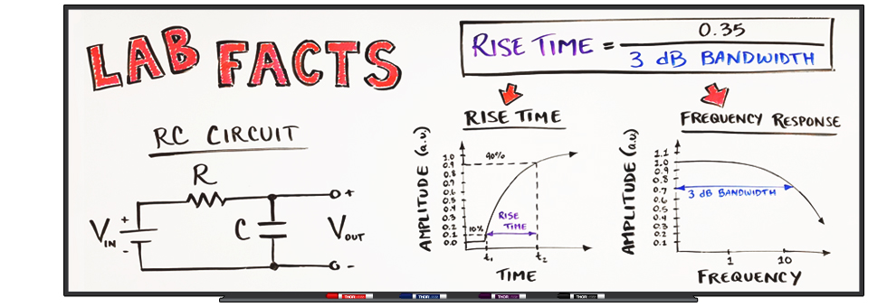
Rise time and 3 dB bandwidth are two closely-related parameters used to describe the limit of a system's ability to respond to abrupt changes in an input signal. Rise time and 3 dB bandwidth are inversely proportional, with a proportionality constant of ~0.35 when the system's response resembles that of an RC low-pass filter. Having a mathematical expression relating the two is useful, since it is possible that only one of these parameters is known or can be found using available resources. Depending on the function of the system and the requirements of the application, it may be most convenient to reference one parameter, the other, or both.
Rise time is measured with respect to time, while 3 dB bandwidth is measured with respect to electrical frequency. Rise time is the time separating two points on the rising edge of the signal output in response to an input step function. The 3 dB bandwidth is found by referencing the system's frequency response. The inversely proportional relationship between rise time and 3 dB bandwidth can be derived by considering the time and frequency response of an ideal RC low-pass filter, which consists of a resistor and capacitor in series.
This Lab Fact uses the RC low-pass filter model to derive the relationship,

where  r is rise time between points 10% and 90% up the rising edge of the output signal, and f3dB is the 3 dB bandwidth. This relationship is valid for many photodiode-based, as well as other first-order, electrical and electro-optical systems. In addition, this Lab Fact provides examples in which rise time or 3 dB bandwidth was measured for photodiode-based systems, with the unmeasured parameter calculated using the relationship between the two parameters.

What is rise time?
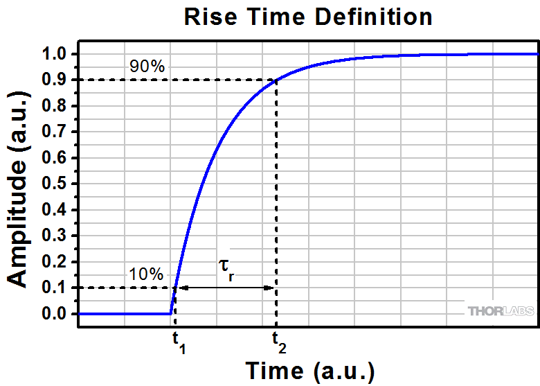
Click to Enlarge
Figure 1.1 Rise time is the time separating two points on the rising edge of a curve. Points located 10% and 90% up the curve are commonly used, although other points are sometimes chosen.
Rise time (r) is the time separating two points on the rising edge of a signal. The points are often located 10% and 90% up the rising edge of the curve, but sometimes other points on the curve are chosen. When the rise time of a system is specified, it describes the fastest response a system can make to an amplitude change in an input signal. If the input signal includes features whose amplitudes change faster than the system can respond, those features will be smoother and broader in the output signal than in the input signal.
How can a system's rise time be measured?
The minimum rise time for a system can be found using an input signal that is first steady at one amplitude and then abruptly steady at a higher amplitude. The jump from the lower to the higher amplitude must happen faster than the system can respond. This type of signal is called a step function. The rising edge of the resulting output signal is used to measure the system's rise time, as illustrated in Figure 1.1.
1
What is the 3 dB bandwidth of a system?
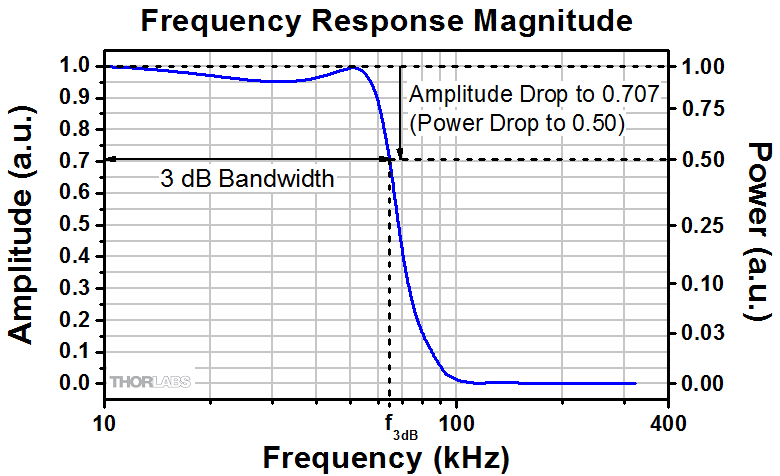
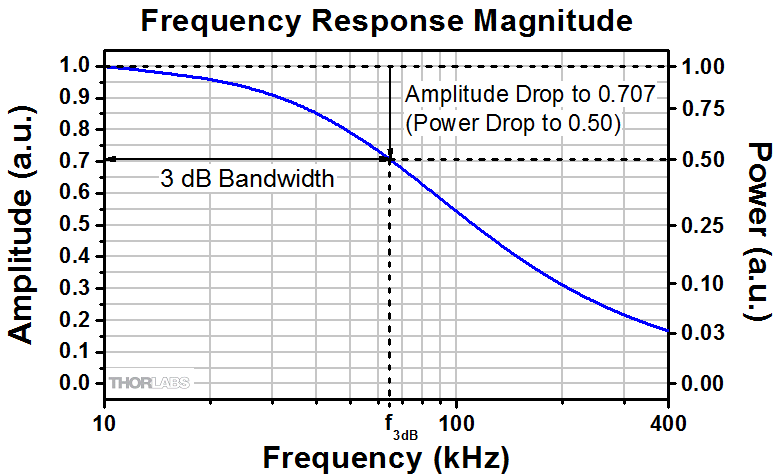
Click to Enlarge
Figure 1.2 The 3 dB bandwidth of an EF124 low-pass electrical filter was measured from 0 Hz to 64.5 kHz. A scaling factor of 0.707 for the amplitude of a voltage or current signal corresponds to a power scaling factor of (0.707)2 = 0.5.
The 3 dB bandwidth is one measure of the range of electrical frequencies a system supports. Input signal frequency components in this range are minorly attenuated by the system, while components outside the 3 dB bandwidth are strongly attenuated. The system's frequency response magnitude data specifies the frequency-dependent scaling factors between input and output signals.
As an example, Figure 1.2 shows the frequency response magnitude data for a low-pass filter that accepts a voltage signal input. Voltage and current signals can be considered in terms of their amplitude or their power. Since the power in one of these signals is proportional to the square of the voltage or current, the power scaling factors are equal to the square of the amplitude scaling factors.
The 3 dB bandwidth specifies the range of frequencies for which the amplitude scaling factors are ≥0.707. This is equivalent to the range over which the power scaling factors ≥0.5. In terms of decibels, a power ratio of 0.5 corresponds to ≥-3 dB. The negative sign is implied in the phrase "3 dB Bandwidth."
The range of input signal components within a system's 3 dB bandwidth dominates the output signal. The output signal is a better representation of the input signal when the 3 dB bandwidth of a system completely overlaps the frequency range of the input signal.
How can a system's 3 dB bandwidth be measured?
The system's bandwidth can be measured using a set of sine waves as input signals. All sine waves should have the same peak-to-peak amplitude, but each should have a different fixed oscillation frequency within the frequency range of interest. It is typical for the lowest oscillation frequency to be close to 0 Hz. For each input sinusoid, the peak-to-peak amplitude of the output signal should be measured. Normalized amplitude scaling factors are obtained by dividing these peak-to-peak measurements by a reference value, which is often the value corresponding to the input signal with the lowest oscillation frequency.
2
When can a system's frequency response be modeled using an RC low-pass filter?

Click to Enlarge
Figure 1.3 Input and ouput signal frequency components typically differ in amplitude and phase, due to system effects.
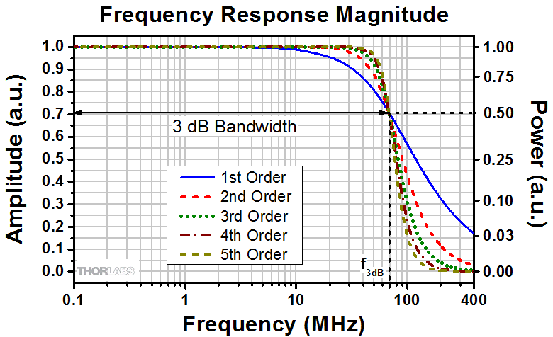
Click to Enlarge
Figure 1.4 The RC low-pass filter circuit is a first-order low-pass filter, which means that the amplitude decreases by a factor of 0.1 when the frequency changes by a factor of 10. Higher order filters have steeper slopes in the vicinity of the cutoff frequency.
A system's frequency response describes the effect the system has on the magnitude and phase of each frequency component in an input signal. Input signal components are often represented as sinusoids oscillating at different fixed frequencies, consistent with Fourier series and Fourier transform representations. Figure 1.3 illustrates a typical example of input and output sinusoidal signal components, which differ in phase and amplitude. The system's effect on the amplitude of each frequency component of the input signal is specified by the system's frequency response magnitude, which was discussed in Card 2.
Systems with frequency response magnitudes similar to those of low-pass filters have frequency-dependent amplitude scaling factors that are significantly larger at lower frequencies than at higher frequencies. With this type of response, a system strongly attenuates components with frequencies above some cutoff frequency (f3dB ). The system's output signal is dominated by the lower frequency components of the input signal.
A low-pass filter can be described by its order, which is determined by the slope of its frequency response magnitude around the cutoff frequency. When the slope of the response decreases at an approximate rate of ω-N, then the filter is an Nth order low-pass filter. Figure 1.4 plots curves corresponding to idealized 1st through 5th order low-pass filters, whose slopes decrease at rates proportional to ω-1 through ω-5, respectively. The low-pass filter whose response is plotted in Figure 1.2 is a 5th order low-pass filter.
The RC low-pass filter is a 1st order low-pass filter, so that the amplitude of its frequency response magnitude at frequency 10ω is approximately 0.1 times the amplitude at frequency ω. This Lab Fact provides equations that are appropriate for use with systems whose frequency response magnitudes are closely similar to that of the 1st order, RC low-pass filter. When a system's response is closely similar to this response, the RC low-pass filter circuit model should provide a reasonable approximation of the system's response. More information about RC low-pass filters and approaches for determining whether system behavior is similar to this filter is presented in the following cards.
It should be noted that the measured frequency response depends not only on the instruments and devices included in the setup, but also on the electrical properties of the cabling and the responses of the read-out instrumentation.
3
What is a convenient model for a low-pass filter?
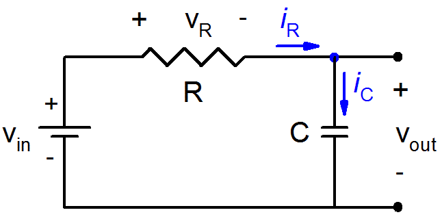
Click to Enlarge
Figure 1.5 The RC low-pass filter circuit is often used as a simple model of low-pass filter behavior. It can be used to derive a relationship between rise time and 3 dB bandwidth.
The RC low-pass filter circuit, shown in Figure 1.5, is often used to model low-pass filter behavior. A voltage source, which can be turned on and off, supplies the input voltage signal (vin ). Terminals on either side of the capacitor (C ) are used to measure the output voltage signal (vout ). Since the resistance across these terminals is infinite, current can only flow through the loop that includes the resistor (R ), capacitor, and voltage source. The result is that the current in the circuit (i ),
 .
. equals the current in the resistor and capacitor arms (iR and iC , respectively). The voltage across the resistor (vR ),
 ,
, is given by Ohm's law and is proportional to the current. The low-pass behavior of the circuit is modeled by considering the changes in voltage and current around the circuit when the input voltage is suddenly switched on, and held at a constant value, after having been turned off for a long time previously. Before switching the voltage source on, no current flowed in the circuit, the capacitor was not charged, and the voltages across the capacitor and resistor were both zero. Switching the voltage on causes current to begin to flow in the circuit, but the flow rate is limited by the capacitor. The current,
 ,
, flows at a rate proportional to the rate at which the voltage across the capacitor (vout ) changes with time (t ). Current flows through the circuit only when vout is changing with time. The sum of voltages around the circuit,
 ,
,and Ohm's law, indicate that when current flow stops, vR drops to zero, and vout is equal to vin . The dynamic changes in current and voltage, from the time the voltage source is turned on to the time current stops flowing, are used to derive the model.
4
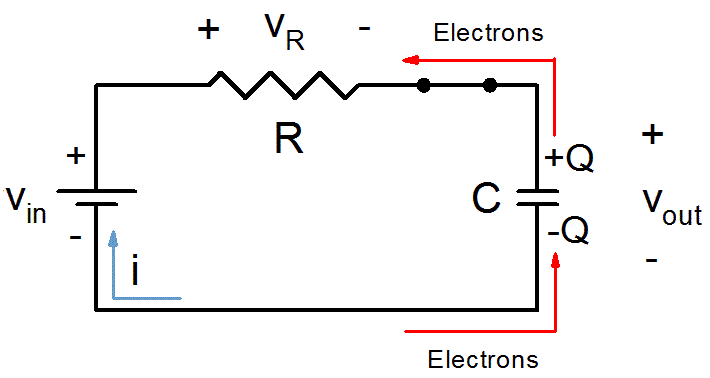
What is a time-dependent equation for the rising edge of a pulse?
Click to Enlarge
Figure 1.6 The rising edge of the output voltage signal from an RC low-pass circuit in response to the sudden application of a constant-voltage input.
Click to Enlarge
Figure 1.7 Electrons accumulate on the bottom plate of the capacitor and flow away from the top plate. The increasing negative and positve charges, (-Q and +Q respectively) result in vout increasing with time. The values of resistance (R ) and capacitance (C ) are constant.
The time-dependent rising edge of the signal shown in Figure 1.6 can be modeled using the RC low-pass circuit illustrated in Figure 1.7. Turning the voltage source on is assumed to result in the supplied voltage immediately jumping from 0 V to a steady value of vin . The sudden push of the supplied voltage causes current to begin to flow in the circuit.
Electrons flow from the negative terminal of the voltage source to the bottom plate of the capacitor. Electrons also flow away from the top plate of the capacitor towards the positive terminal of the voltage source. Since charged particles cannot flow through the capacitor, electrons accumulate on the bottom plate of the capacitor, and the number of electron vacancies on the top plate of the capacitor increase, as more electron flow.
A negative charge (-Q ) accumulates on the bottom plate of the capacitor, while an equal amount of positive charge (+Q ) builds up on the top plate. The separated positive and negative charges result in a voltage, vout , developing across the capacitor that is proportional to the magnitude of the total charge on one of the plates (Q ). This voltage increases as long as the current continues to flow.*
The rate at which charge accumulates on the plates is highest when the source voltage first turns on, and this is also when vout is increasing the fastest. The flow of the charged particles is opposed by vout , and as this voltage becomes larger, the rate at which charge accumulates on the capacitor's plates becomes slower. When vout and vin are equal, the flow of current stops.
This description of how vout changes in response to a step function input voltage agrees with the curve plotted in Figure 1.6. The mathematical expression for this behavior,
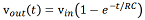 ,
,is derived in the full report using the equations presented in Card 4.
*Note that current is defined to flow in the direction opposite the flow of electrons. The direction of current flow is indicated by the blue arrow in Figure 1.7.
5
What is a frequency-dependent equation for the amplitude scaling factors?
Click to Enlarge
Figure 1.8 The RC low-pass filter circuit is often used as a simple model of low-pass filter behavior. It can be used to derive a relationship between rise time and 3 dB bandwidth.
The circuit shown in Figure 1.8 and the equations presented in Card 4 can also be used to derive an expression for the frequency response. Since the frequency response describes the relationship between input and output signals, and the system defines that relationship, the method involves describing the frequency-dependent ratio of vout to vin entirely as a function of system components.
This approach, which is detailed in the full report, results in a complex-valued expression for frequency response (H ) that describes the effect the system has on both the phase and magnitude of each input signal component, for an arbitrary input signal. The frequency response magnitude, which is the absolute value of the frequency response (|H | ), provides the amplitude scaling factors.
The derivation shows that the amplitude of each frequency component input to an RC low-pass filter is scaled by a factor,
which is dependent only on the frequency (f ) of the input signal component, resistance (R ), and capacitance (C ). The power scaling factors (|H |2 ) can be found by squaring this equation for amplitude scaling factors,
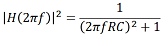 .
.6
What is the final step for relating rise time and 3 dB bandwidth?
Click to Enlarge
Figure 1.9 Rise time is the time separating two points on the rising edge of a curve. Points located 10% and 90% up the curve are commonly used, although other points are sometimes chosen.
First, find an expression for rise time.
The time-dependent equation for the rising edge of a pulse,
,was used to find a relationship between rise time and the RC product. The relationship was found by referencing Figure 1.9 and noting that the amplitude at t1 is 0.1, the amplitude at t2 is 0.9, and the amplitude at infinite time is 1. These amplitude values and the defintion for rise time (t2 - t1 ) were used to find an expression,
 ,
, which includes only rise time and the RC product.
Second, find an expression for the 3 dB bandwidth.
The frequency-dependent equation for the power scaling factors,
Click to Enlarge
Figure 1.10 The 3 dB bandwidth of the RC low-pass electrical filter, which is a first-order low-pass filter. An amplitude scaling factor of 0.707 corresponds to a power scaling factor of (0.707)2 = 0.5.
,was used to find a relationship between the 3 dB bandwidth (f3dB ) and the RC product. As illustrated by Figure 1.10, at the upper-frequency boundary of the 3 dB bandwidth, the power scaling factor is half the maximum value. When the left-hand side of the equation is set to 0.5, the resulting expression,
 ,
, relates the 3 dB bandwidth and the RC product.
Then, combine both expressions to eliminate the RC constant.
The results of the first and second steps, can be combined to find an expression that relates the rise time and 3 dB bandwidth to each other. This expression,
, is a convenient way to estimate rise time when the 3 dB frequency is known, or vice versa.
Since this relationship was derived using a low-pass filter model, it is intended to be used only when the system behaves like a low-pass filter. Due to it being unlikely that the ideal RC low-pass filter circuit perfectly models the behavior of the system under consideration, this expression is useful for estimating parameters of real systems but should not be expected to provide exact results. When accurate values are needed, the parameter of interest should be directly measured. If both parameters are needed, but only one can be measured, the other can be calculated using rigorous Fourier transform-based techniques.
7
What is an example of 3 dB bandwidth estimated from rise time?
Photodiode-based systems often include a load resistor, which is used to convert the current signal from the photodiode to a voltage signal that can be more easily measured. The choice of load resistor value impacts several aspects of system performance, including the rise time and 3 dB bandwidth. Measurements of rise time were made for a photodiode-based system, and the value of load resistance was different for each measurement. Two of the measured rise time curves are plotted in Figures 1.11 and 1.12. During this work, the system's 3 dB bandwidth was also required. The expression,
,would provide a reasonable estimate of the 3 dB bandwidth value, if the rising edges of signals output from this system and from an RC low-pass circuit were similar. The expression for the rising edge of a signal output by an RC low-pass circuit,
,was used to calculate the red curves shown in Figures 1.11 and 1.12. As the curves provide a reasonable fit for the data, the expression at the top of this card was used to calculate estimates of the system's 3 dB bandwidth for the cases of different effective load resistances. The measured rise times and estimated values of 3 dB frequency are listed in Table 1.13.
These two parameters have a reciprocal relationship, so that an increase in the system's rise time corresponds to a decrease in the system's bandwidth. When some of the frequencies in the input signal exceed the system's bandwidth, the system attenuates these higher frequencies. This results in an output signal with features that are more rounded and broader than the same features in the input signal. This is illustrated by Figures 1.11 and 1.12, which should ideally have a vertical rising edge, but instead have rising edges with slopes that become shallower as the rise time increases (and the bandwidth decreases).
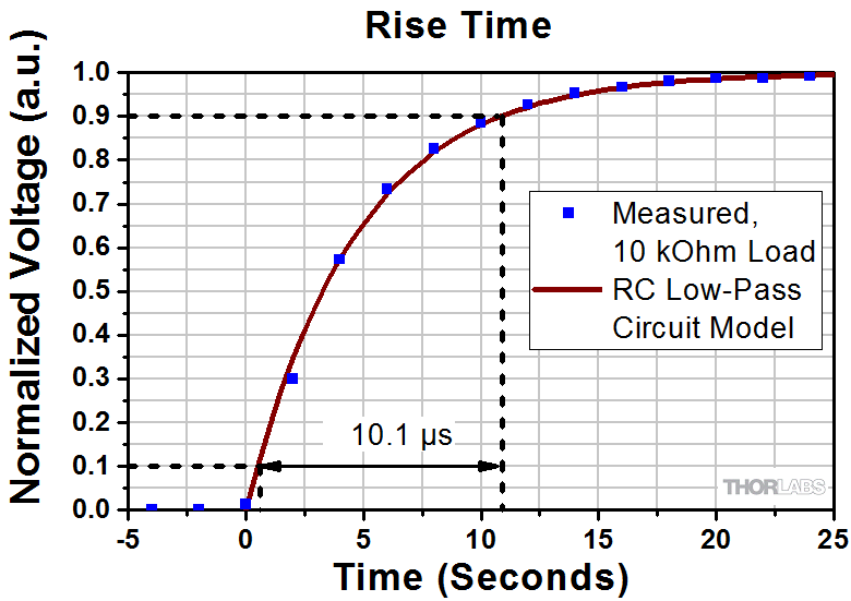
Click to Enlarge
Figure 1.11 The rise time measured for a photodiode-based system with a 10 kΩ effective load resistance was 10.1 µs. The rising edge calculated using the RC low-pass filter model (red curve) is a good fit for the data.
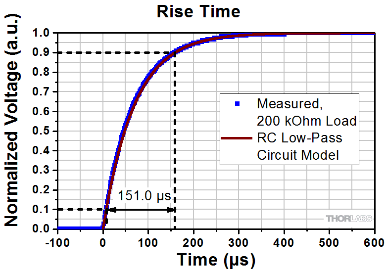
Click to Enlarge
Figure 1.12 The rise time measured for a photodiode-based system with a 200 kΩ effective load resistance was 151.0 µs. The rising edge calculated using the RC low-pass filter model (red curve) is a good fit for the data.
| Table 1.13 3 dB Bandwidth Estimated from Rise Timea | ||
|---|---|---|
| Effective Load Resistance | Measured Rise Time | Calculated 3 dB Bandwidth |
| 10 kΩ | 10.1 µs | 34.7 kHz |
| 200 kΩ | 151.0 µs | 2.3 kHz |
8
What is an example of rise time estimated from 3 dB bandwidth?
The performance of photodiode-based systems are also affected by the reverse bias voltage applied across the photodiode. The effect of the reverse bias voltage on the system response was investigated for a system whose response was faster than that of the system tested in the previous examples. In this case, the rise times were on the order of nanoseconds, which can be challenging to measure. Instead of measuring rise time directly, the magnitude of the system's frequency response was measured, and the rise times were estimated from these data using the expression,
.The measurements are plotted as points in Figures 1.14 and 1.15, and the expression,
was used to model the response of the corresponding RC low-pass filters, which are plotted as the red curves in each figure. Since there is a close fit between the modeled and measured responses, the expression at the top of this card was expected to provide a good estimate of the rise time of this system for the different cases of reverse-bias voltage. Table 1.16 lists the measured 3 dB bandwidths and the rise times estimated from them.
These measurements show that increasing the reverse-bias voltage across the photodiode was effective in increasing the 3 dB bandwidth of the system. As the 3 dB bandwidth increased, the rise times decreased. This would increase the rate at which the system could respond to abrupt changes in the input signal, which would enable the system to better reproduce the input signal's narrow and quickly changing amplitude features in the output signal. However, there is a limit to the increase in bandwidth that can be obtained using this approach, since an excessively high reverse-bias voltage will damage the photodiode.
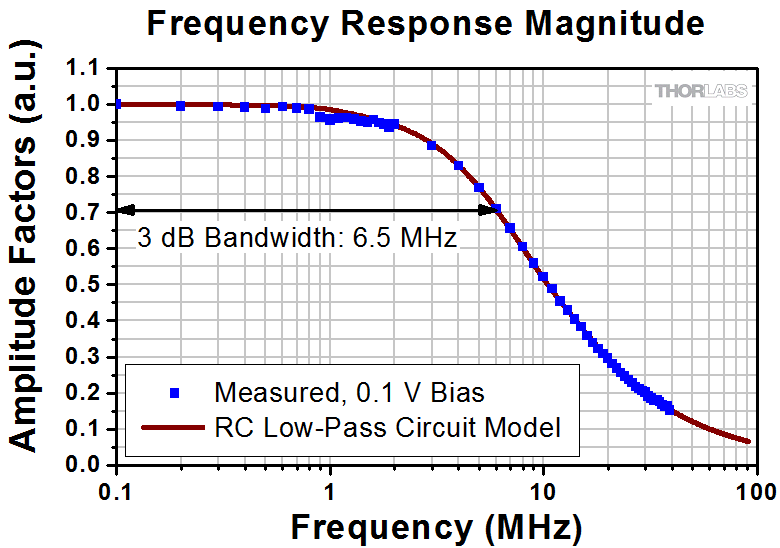
Click to Enlarge
Figure 1.14 The 3 dB bandwidth measured for a system with a 0.1 V reverse bias across the photodiode was 6.5 MHz. The frequency response calculated using the RC low-pass filter model (red curve) is a good fit for the data.

Click to Enlarge
Figure 1.15 The 3 dB bandwidth measured for a system with a 3 V reverse bias across the photodiode was 14.1 MHz. The frequency response calculated using the RC low-pass filter model (red curve) is a good fit for the data.
| Table 1.16 Rise Time Estimated from 3 dB Bandwidth | ||
|---|---|---|
| Bias Voltage | Measured 3 dB Bandwidth | Calculated Rise Time |
| 0.1 V | 6.5 MHz | 54.1 ns |
| 3.0 V | 14.1 MHz | 24.7 ns |
9
Additional Information
Interested in products related to this work?
- CLD1010LP Mount, Current, and Temperature Controller for FIber-Pigtailed Laser Diodes
- Fiber-Pigtailled 980 nm Laser Diodes
- VOA980-FC Variable Optical Attenuator
- DET02AFC 1 GHz FC/PC-Coupled Photodetector
Want more information about how a system's rise time and 3 dB bandwidth affect distortion in square waves and rectangular pulse trains?
Visit the Lab Fact webpage, or download the detailed report.
Want to read more Lab Facts or some of Thorlabs' other technical publications?
Browse the visual navigation guide.
10
| Posted Comments: | |
| No Comments Posted |