 Products Home
Camera Basics
Ultra-Compact CMOS Cameras
with Low Read Noise
Passively Cooled, Compact
CMOS Sensor Cameras
with Low Read Noise
Actively Cooled, Monochrome sCMOS
Camera with Lowest Read Noise
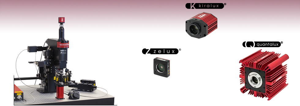
Kiralux® 1.3 Megapixel Monochrome CMOS Camera in Thorlabs' Bergamo® II Multiphoton Microscope, with Drosophila VR Theater Stage

Please Wait
Table of Contents
Sensor Properties
- Quantum Efficiency and Spectral Sensitivity
- Camera Noise and Sensor Temperature
- CCD Camera Readout
Optical System
- Imager Size and Field of View
- Resolution
- Vignetting
System Integration
- Camera Interfaces
- Triggered Operation
Applications
An Introduction to Camera Terminology and Options
This page is designed to introduce terminology that is useful when choosing a scientific camera. It is split into four sections. Sensor Properties and Optical System discuss the various specifications and terms used to describe scientific cameras. These tabs explain how to use the specifications to choose the correct camera for your experiment, and also provide example calculations for our scientific camera product line. System Integration details features that allow Thorlabs' scientific cameras to be integrated with other laboratory instrumentation. Finally, Applications contains sample images and discussions of research enabled by our scientific cameras.

Questions?
If you have any questions about cameras, or would like to discuss a particular application, please click the Contact Us button.Sensor Properties
Click to Enlarge
Click for Raw Data
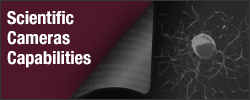
Figure 1: The QE curve for our previous-generation monochrome 1.4 megapixel camera; the QE curves for all of our scientific cameras are in the table below. The NIR Enhanced (Boost) Mode is available on the 1.4 megapixel camera and can be selected via the software. The IR blocking filter should also be removed for maximum NIR sensitivity. For more information on Boost mode, please see the Imaging in the NIR section.
Quantum Efficiency and Spectral Sensitivity
A camera sensor, such as a CCD or CMOS, converts incident light into an electrical signal for processing. This process is not perfect; for every photon that hits the sensor there will not necessarily be a corresponding electron produced by the sensor. Quantum Efficiency (QE) is the average probability that a photon will produce an electron, and it is expressed as a conversion percentage. A camera with a higher quantum efficiency imager will require fewer photons to produce a signal as compared to a camera with lower quantum efficiency imager.
Quantum efficiency is dependent on the properties of the material (e.g. silicon) upon which the imager is based. Since the wavelength response of the silicon is not uniform, QE is also a function of wavelength. QE plots are provided in Figure 1 and the summary table below so that the quantum efficiency of different cameras can be compared at the wavelengths of the intended application. Note that the interline CCDs that are used in scientific cameras typically have a microlens array that spatially matches the pixel array. Photons that would otherwise land outside of the photosensitive pixel are redirected onto the pixel, maximizing the fill factor of the sensor. The QE plots shown here include the effects of the microlens arrays.
IR Blocking Filters and AR-Coated Windows
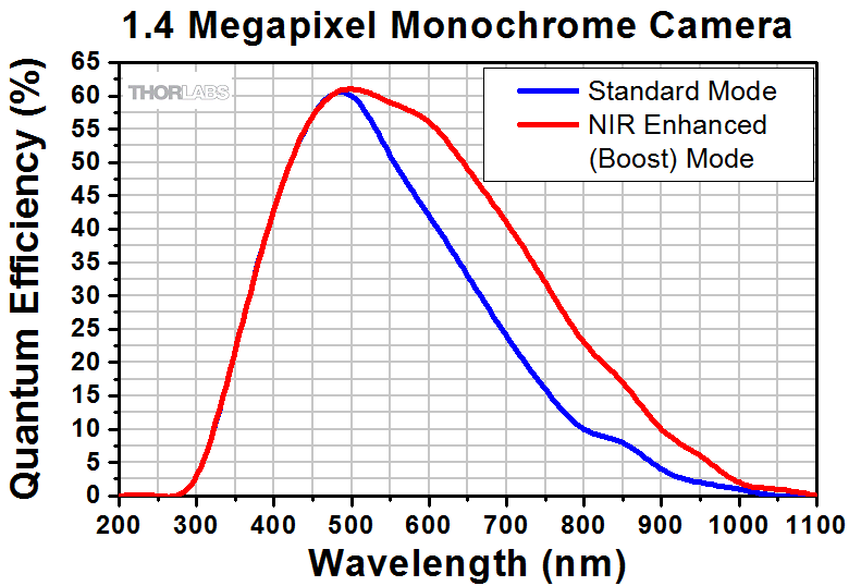
Various techniques can be used to either limit or enhance the sensitivity at various wavelength ranges. The response of a silicon detector extends into the Near Infrared (NIR) region; in most applications it is important for the response of the camera to closely approximate the human-eye response. For this reason, an IR blocking filter that blocks the signal above 700 nm is typically installed in front of the silicon detector. Alternatively, an AR-coated window with a low reflectance over the visible range may be installed in the camera instead. In Thorlabs' scientific cameras, these optics (if present) are removable to allow imaging in the NIR or UV region of the spectrum, or they can be replaced with a different filter to match the specific requirements of the user's application. See the summary table below for the details on the removable optics included in our cameras. The filter removal process for our scientific CCD cameras is shown in Figures 2 through 4. For details on how to remove the optics in our CMOS cameras, please see the respective manuals.
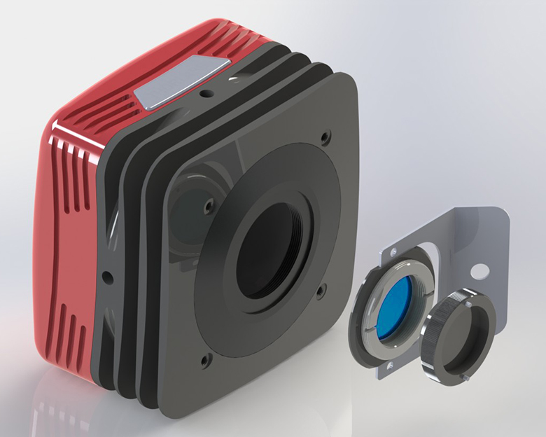
Click to Enlarge
Figure 2: Exploded view of a Thorlabs' scientific CCD camera optical and mechanical components.
Click to Enlarge
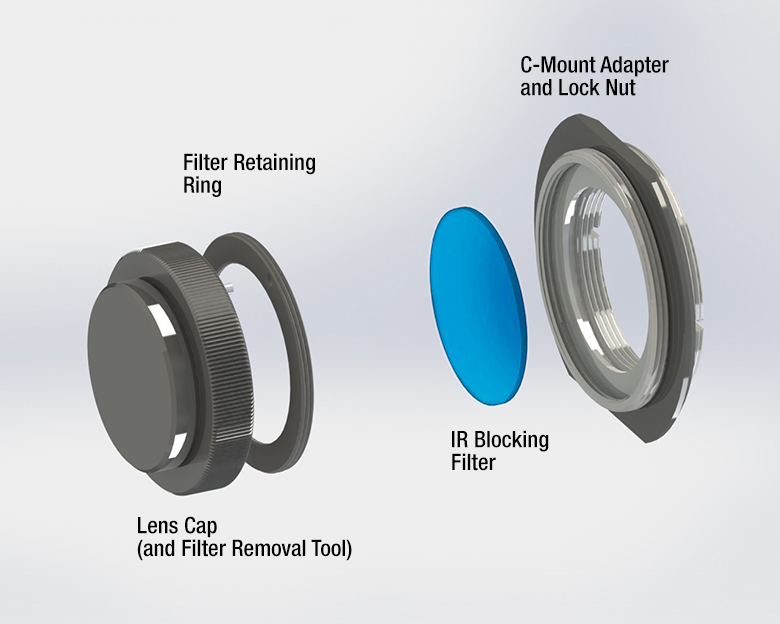
Figure 4: The filter housing can be removed by completely unscrewing the C-mount adapter and lock nut with the wrench.
Click to Enlarge
Figure 3: The lens cap functions as a tool that can loosen the retaining ring holding the IR blocking filter in place. The filter can be replaced with any user-supplied Ø1" (25 mm) filter or other optic up to 4 mm thick. Removal instructions are provided in chapter 4 of the camera user's manual.
Imaging in the NIR
Our previous-generation 1.4 megapixel monochrome CCD cameras have a software-selectable NIR Enhanced (Boost) mode. While the response of silicon generally limits the use of CCD and CMOS cameras at longer wavelengths, a camera operating in Boost mode can have enough sensitivity up to the 900 - 1000 nm range to acquire usable images for many applications. These include applications such as NIR beam-profiling where the intensity of illumination is often quite bright; in other low-light NIR applications the low noise of the 1.4 megapixel sensor allows long exposures with sufficient signal-to-noise ratio (see below for more details on SNR). In addition, we offer our CS135MUN 1.3 MP CMOS camera, which features an NIR-Enhanced CMOS sensor and <7.0 e- RMS read noise for low-light imaging applications.
Quantum Efficiency Summary
| Camera Family | Sensor Type | Peak Quantum Efficiency | Quantum Efficiency Plots | Removable Optic | |
|---|---|---|---|---|---|
| Compact Scientific Cameras | |||||
| Kiralux® 1.3 MP CMOS Cameras | Monochrome CMOS | 59% at 550 nm | Window, Ravg < 0.5% per Surface (400 - 700 nm) | ||
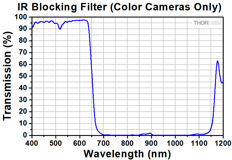
| Color CMOS | See Quantum Efficiency Plot | 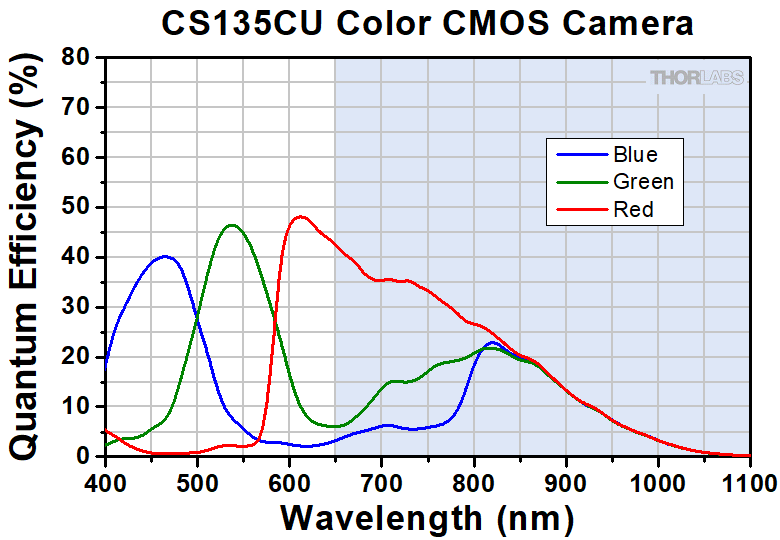 |
IR Blocking Filter (Click Here for Graph) | ||
| NIR-Enhanced CMOS | 60% at 600 nm | Window, Ravg < 0.5% per Surface (650 - 1050 nm) | |||
| Zelux® 1.6 MP CMOS Cameras | Monochrome CMOS | 69% at 575 nm | Window, Ravg < 0.5% per Surface (400 - 700 nm) | ||
| Color CMOS | 65% at 535 nm |  |
IR Blocking Filter (Click Here for Graph) | ||
| Quantalux® 2.1 MP sCMOS Cameras | Monochrome sCMOS | 61% at 600 nm | Window, Ravg < 0.5% per Surface (400 - 700 nm) | ||
| Kiralux 2.3 MP CMOS Cameras | Monochrome CMOS | 78% at 500 nm | Window, Ravg < 0.5% per Surface (400 - 700 nm) | ||
| Color CMOS | See Quantum Efficiency Plot | 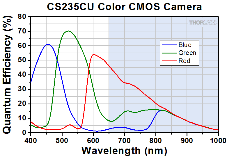 |
IR Blocking Filter (Click Here for Graph) | ||
| Kiralux 5 MP CMOS Cameras | Monochrome CMOS | 72% (525 - 580 nm) | Window, Ravg < 0.5% per Surface (400 - 700 nm) | ||
| Color CMOS | See Quantum Efficiency Plot |  |
IR Blocking Filter (Click Here for Graph) | ||
| Kiralux 5 MP CMOS Polarization Camera | Monochrome CMOS with Wire Grid Polarizer Arraya |
72% (525 - 580 nm) | Window, Ravg < 0.5% per Surface (400 - 700 nm) | ||
| Kiralux 8.9 MP CMOS Cameras | Monochrome CMOS | 72% (525 - 580 nm) | Window, Ravg < 0.5% per Surface (400 - 700 nm) | ||
| Color CMOS | See Quantum Efficiency Plot |  |
IR Blocking Filter (Click Here for Graph) | ||
| Kiralux 12.3 MP CMOS Cameras | Monochrome CMOS | 72% (525 - 580 nm) | Window, Ravg < 0.5% per Surface (400 - 700 nm) | ||
| Color CMOS | See Quantum Efficiency Plot |  |
IR Blocking Filter (Click Here for Graph) | ||
More Information
For a detailed review of camera noise, SNR, and the effects of sensor temperature, including sample calculations, please see our complete tutorial.

Camera Noise and Sensor Temperature
When purchasing a camera, it is important to consider the intended application and its "light budget." For bright light situations, it is sufficient to choose a camera that has an adequately high quantum efficiency and then consider other factors, such as sensor format, frame rate, and interface. For low light situations, it is important to consider quantum efficiency as well as read noise and dark current, as described below.
Sources of Noise
If several images are taken of the same object under the same illumination, there will still be variation in the signal recorded by each pixel. This "noise" in a camera image is the aggregate spatial and temporal variation in the measured signal, assuming constant, uniform illumination. There are several components of noise:
- Dark Shot Noise (σD): Dark current is a current that flows even when no photons are incident on the camera. It is a thermal phenomenon resulting from electrons spontaneously generated within the silicon chip (valence electrons are thermally excited into the conduction band). The variation in the amount of dark electrons collected during the exposure is the dark shot noise. It is independent of the incident light level but is dependent on the temperature of the sensor. Since the dark current decreases with decreasing temperature, the associated dark shot noise can be decreased by cooling the camera.
- Read Noise (σR): This is the noise generated in producing the electronic signal, mainly due to errors in measuring the electrons at the read amplifier. This results from the sensor design but can also be impacted by the design of the camera electronics as well as the gain setting. It is independent of signal level and temperature of the sensor, and is larger for faster CCD pixel clock rates.
- Photon Shot Noise (σS): This is the statistical noise associated with the arrival of photons at the pixel. Since photon measurement obeys Poisson statistics, the photon shot noise is dependent on the signal level measured. It is independent of sensor temperature. If the photon shot noise is significantly higher than the dark shot noise, then cooling provides a negligible benefit in terms of the noise.
- Fixed Pattern Noise (σF): This is caused by spatial non-uniformities in efficiency of the pixels and is independent of signal level and temperature of the sensor. Note that fixed pattern noise will be ignored in the discussion below; this is a valid assumption for our scientific CCD cameras but may need to be included for other non-scientific-grade sensors.
Image quality (as represented by the Signal-to-Noise [SNR] ratio) is the ratio of:
- The number of signal electrons, which may be estimated to be the product of:
- The light level, represented by the photon flux in photons/sec,
- The duration of exposure (seconds),
- And the Quantum Efficiency (QE).
- To the number of noise electrons, which may be estimated to be the quadrature sum of:
- The photon shot noise,
- The read noise,
- And the dark shot noise.
Photon-derived signal electrons cannot be distinguished from the noise electrons that are generated during image formation, readout, and digitization. SNR is a convenient "figure of merit" to evaluate how well the signal electrons overcome the noise electrons in the system under a particular set of conditions. It provides a way to quantitatively compare the images, because a higher SNR usually correlates with an observable improvement in image quality. Complete details on calculating SNR can be found in the Camera Noise Tutorial.
| Exposure | Camera Recommendation |
|---|---|
| <1 s | Standard Non-Cooled Camera Generally Sufficient |
| 1 s to 5 s | Cooled Camera Could Be Helpful |
| 5 s to 10 s | Cooled Camera Recommended |
| >10 s | Cooled Camera Usually Required |
Bright Light Imaging
Bright light conditions are considered "shot-noise limited," which means that photon shot noise is the dominant source of noise and dark current is negligible. Due to this, the SNR is proportional to the square root of the signal, as shown in the complete tutorial, and therefore increasing the exposure will not have as large an effect on image quality. In this case, one can use any sensor with sufficiently high QE. Other considerations such as imager size, package size, cost, interface, shutter, trigger, accessories, and software may be more significant to the selection process. TE cooling is usually not required because the exposure duration is short enough to ensure that dark shot noise is minimal.
Low Light Imaging
Low light conditions may be considered "read noise limited," which means that photon-generated electrons have to overcome the read noise in the sensor, all other sources of sensor noise being negligible under these conditions. In this case, the signal-to-noise ratio will have a linear relationship with the exposure duration, and therefore low-light images taken with longer exposures will look noticeably better. However, not all applications can tolerate long exposures; for example, if there are rapid changes of intensity or motion in the field of view. For low light images, it helps to have an imager with low read noise, high QE, and low dark current. It is for these reasons we recommend our Scientific CCD or sCMOS Cameras for low light applications. TE cooling can be beneficial when the duration of exposure exceeds approximately 3 to 5 seconds.
Other Considerations
Thermoelectric cooling should also be considered for long exposures even where the dark shot noise is not a significant contributor to total noise because cooling also helps to reduce the effects of hot pixels. Hot pixels cause a "star field" pattern that appears under long exposures. Sample images taken under conditions of no light, high gain, and long exposure can be viewed in the tutorial.
Click to Enlarge
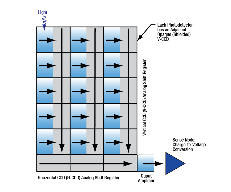
Figure 5: Schematic showing the process for charge transfer and readout of an interline CCD.
This animation details how charge is accumulated on the pixels of an interline CCD, how those charges are shifted, and then read out as the next exposure begins.
CCD Camera Readout
Our scientific CCD cameras are based on interline CCD sensors. This sensor architecture and readout is illustrated in Figure 5 as well as the animation to the lower right. An interline CCD may be visualized as a device that develops a 2D matrix of electronic charges on a horizontal and vertical (H x V) pixel array. Each pixel accumulates a charge that is proportional to the number of incident photons during an exposure period. After the exposure period, each element of the charge matrix is laterally shifted into an adjacent element that is shielded from light. Stored charges are clocked, or moved, vertically row-by-row into a horizontal shift register. Once a row of charges is loaded onto the horizontal shift register, charges are serially clocked out of the device and converted into voltages for the creation of an analog and/or digital display. An advantage of this architecture is that once the charges are shifted into the masked columns, the next exposure can immediately begin on the photosensitive pixels.
ThorCam, our camera control and image acquisition software, allows users to switch freely between combinations of readout parameters (clock rate, number of taps, binning, and region of interest) and select the combination that works best for the particular application. These readout options are described in the following sections.
Readout Clock Rate
In Figure 5 a simplified CCD pixel array is shown as a 5 x 3 grid. The simplified horizontal readout register is therefore 1 x 3. The triangle at the end of the horizontal shift register represents the "sense node" where charges are converted into voltages and then digitized using an analog-to-digital converter. The physics of the device limit the rate at which image frames can be "read out" by the camera.
Our scientific cameras operate at 20 or 40 MHz readout, which is the rate at which the pixels are clocked off of the shift register. The readout rate determines the maximum frame rate of the camera. Going from 20 MHz to 40 MHz will nominally double the frame rate of the camera, at the expense of slightly higher read noise, assuming all other parameters remain the same. There will be slightly higher read noise associated with the 40 MHz readout, but if there is plenty of light in the field of view, then the image is shot-noise limited, not read-noise limited. In shot-noise limited cases, the 40 MHz readout mode results in a speed increase without any penalty.
Multi-Tap Operation
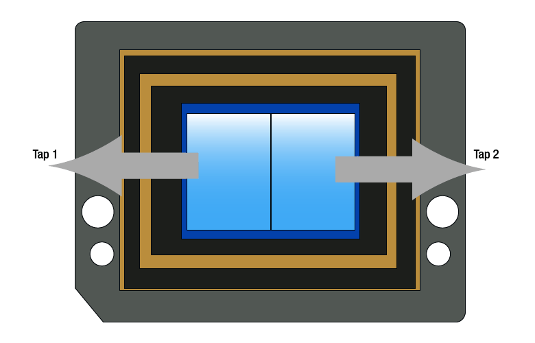
One way to further increase the frame rate is to divide the CCD into sections, each with its own output "tap," or channel. These taps can be read out independently and simultaneously, decreasing the total time it takes to read out the pixels, and thus increasing the total frame rate. Many of the chips used in our cameras can be operated as single-tap (illustrated in the animation), dual-tap (shown in Figure 6), or quad-tap (shown in Figure 7) operation.
Single Tap Readout
Figure 5 and the animation to the right show the horizontal readout register at the bottom of the CCD. Horizontal clocking of charges out of the horizontal register at a sense node, followed by charge to voltage conversion using an analog-to-digital converter are rate-limiting steps, and thus limit the maximum frame rate of the camera.
In conventional (single tap) readout mode, each row of charges is loaded onto the horizontal register and clocked out towards the sense node, at a rate determined by the readout clock rate of 20 or 40 MHz.
Dual Tap Readout
As shown in Figure 6, the sensor (and the horizontal shift register) has been split in two and there are two sense nodes, one on either end of the shift register. During readout, each row of charges is loaded onto the horizontal register (just as in the conventional single tap case). However, half of the pixels in each row are clocked out towards the left and the other half are clocked out to the the right towards the sense nodes and their respective analog-to-digital converters. This allows the charges to be clocked out in half the time of the single tap mode. The image halves are digitally reconstructed, so that the viewer sees a normal image, reconstituted from the two half images. Since the charges go through two different sense nodes and analog-to-digital converters, there can be a slight mismatch between the two halves; this can be dependent on the image content and camera exposure, gain, and black level settings. Although there are methods implemented to mitigate the effect of this mismatch over a wide operating range, there can be a vertical "seam" that is discernable in the center of the image.
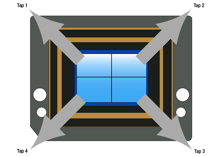
Quad Tap Readout
As shown in Figure 7, the sensor has been split in four quadrants; there are now two horizontal shift registers, one at the top and one at the bottom of the chip. The vertical charge transfer is split with the top half of rows shifted upwards and the lower half of rows shifted downwards. During readout, each row of charges is loaded onto the horizontal registers, each of which has a sense node and analog-to-digital converter at each end. As in the case of dual-tap readout, half of each row of pixels are clocked out towards their sense node and onto their respective analog-to-digital converter. This allows the charges to be clocked out in a quarter of the time of single-tap mode. The image quarters are digitally reconstructed, so that the user sees a normal image reconstituted from the four quarter images. Since the charges go through four different sense nodes and analog-to-digital converters there can be a slight mismatch between the four quarters. The mismatch can be dependent on the image content and camera exposure, gain, and black level settings. Although there are methods implemented to mitigate the effect of this mismatch over a wide operating range, there can be vertical and horizontal "seams" that are discernable in the center of the image.
The summary table below the figures details the number of taps for each camera family. Each camera family webpage has a table with the maximum frame rate specifications for each readout rate and tap combination. The number of taps is user-selectable in the ThorCam software settings.
Click to Enlarge
Figure 6: Dual-Tap Camera Illustration
Click to Enlarge
Figure 7: Quad-Tap Camera Illustration
Multi-Tap Readout Operation Summary
Region of Interest (ROI)
In sub-region readout, which is also known as Region of Interest (ROI) mode, the camera reads out only a subset of rows selected by the user and achieves a higher effective frame rate. In the ThorCam application software, this area is selected by drawing an arbitrary rectangular region on the display window. The unwanted rows above and below the ROI are fast-scanned and are not clocked out, while the desired rows are clocked out normally. Unwanted columns are trimmed in the software. While the spatial resolution of the image is maintained, the field of view is reduced.
Since changing the ROI affects the number of CCD rows read out (not columns), only the vertical ROI dimension affects the frame rate; changing the horizontal ROI dimension will have no effect on the frame rate. The resulting frame rate is not a linear function of the ROI size since there is some additional time involved to fast-scan the unwanted rows as well as to read out the desired ROI.
Binning
In Binning mode, a user-selectable number of adjacent horizontal and vertical pixels on the CCD are effectively read out as a single pixel. Increasing the binning reduces the spatial resolution but increases the sensitivity and frame rate of the camera as well as the signal-to-noise ratio of the resulting image. While the speed, sensitivity, and SNR are improved, the spatial resolution of the image is reduced.
Binning and ROI modes can be combined to optimize readout and frame rate for the particular application.
Optical System
Imager Size and Field of View
In the following discussion, we will focus on calculating the field of view for an imaging system built using microscope objectives; for information about field of view when using machine vision camera lenses please see our Camera Lens Tutorial.
In a microscope system, it is important to know how the size of the camera sensor will affect the area of your sample that you are able to image at a given time. This is known as the imaging system's field of view. It is calculated by taking the sensor's dimensions in millimeters and dividing it by the imaging system's magnification. As an example, our previous-generation 8 MP CCD sensor has an 18.13 mm x 13.60 mm array; at a 40X magnification, this corresponds to a 457 µm x 340 µm total area at the sample plane.
Choosing the imager size must also be balanced against the other parameters of the sensor. Generally, as sensor size increases, the maximum frame rate decreases.
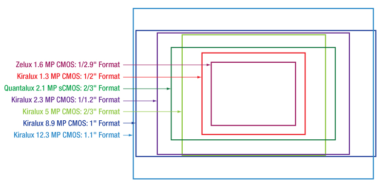
Camera sensor sizes are given in terms of "format." The format designations are expressed in fractional inches and represent the outer diameter of the video tube that has an imaging diagonal closest to the diagonal of the digital sensor chip. These sizes are not completely standardized, and therefore some variation exists between the exact sizes, and occasionally even aspect ratios, with the same format from different manufacturers. Figure 1 shows the approximate sensor sizes for our scientific cameras.
Click for Details
Figure 1: An illustration of relative sensor sizes and aspect ratios for our scientific cameras; please refer to the table to the left for specific dimensions.
The summary table below lists the format and sensor size for all of our scientific cameras in pixels and millimeters.
| Camera Family | Format (Diagonal) |
Resolution (pixels) |
Pixel Size (µm) |
Sensor Size (mm) |
|---|---|---|---|---|
| Zelux® 1.6 MP CMOS | 1/2.9" (6.2 mm) | 1440 x 1080 | 3.45 x 3.45 | 4.97 x 3.73 |
| Kiralux® 1.3 MP CMOS | 1/2" (7.76 mm) | 1280 x 1024 | 4.8 x 4.8 | 6.14 x 4.92 |
| Quantalux® 2.1 MP sCMOS | 2/3" (11 mm) | 1920 x 1080 | 5.04 x 5.04 | 9.68 x 5.44 |
| Kiralux 5 MP CMOS | 2/3" (11 mm) | 2448 x 2048 | 3.45 x 3.45 | 8.45 x 7.07 |
| Kiralux 5 MP Polarization CMOS | ||||
| Kiralux 2.3 MP CMOS | 1/1.2" (13.4 mm) | 1920 x 1200 | 5.86 x 5.86 | 11.25 x 7.03 |
| Kiralux 8.9 MP CMOS | 1" (16 mm) | 4096 x 2160 | 3.45 x 3.45 | 14.13 x 7.45 |
| Kiralux 12.3 MP CMOS | 1.1" (17.5 mm) | 4096 x 3000 | 3.45 x 3.45 | 14.13 x 10.35 |
Resolution
It is a common misconception to refer to the number of pixels (H x V) as the resolution of a camera. More accurately, the resolution is the optical resolution: the ability to resolve small features. In the following discussion, we will focus on imaging systems which use microscope objectives; for information about building a system with machine vision camera lenses please see our Camera Lens Tutorial.
Calculating the Resolution of an Imaging System
In an imaging system, there is a finite limit to how close objects can be in order to be distinguished. Within an imaging system designed to limit aberrations, such as a high-quality microscope, the only limit on the resolution will be due to diffraction. The image at the focal plane can be thought of a collection of independent, overlapping diffraction patterns from each point on an object. Two adjacent points can be thought of as resolved when the central maximum, or Airy disk, of one diffraction pattern is in the first minimum of another. This condition is known as the Rayleigh Criterion, and can be expressed as:
R=1.22λ/(2NA),
where R is the distance between the two Airy disks, λ is the wavelength of light, and NA is the numerical aperture of the microscope's objective. For example, with a 0.75 NA objective, the resolution for 550 nm light will be (1.22*550 nm)/(2*0.75) = 0.45 µm.
Determining Necessary Camera Pixel Size
The microscope objective will also have a magnification; this value indicates the amount of enlargement of the sample at the image plane. For example, a 2X objective will form an image that is twice the size of the object. If you are using a 0.75 NA, 40X objective, the resolution limit at the sample for 550 nm light will be 0.45 µm (as calculated above). A feature with a length of 0.45 µm in the sample will be magnified by a factor of 40 in the image, so that the feature at the image plane will be 17.9 µm long.
In order to accurately represent the image on the discrete imaging array of the CCD or CMOS camera, it is necessary to apply the Nyquist criterion, which states that the smallest resolvable feature of the image needs to be sampled by the sensor at twice this rate; put another way, there needs to be (at least) two pixels to capture each optically resolvable feature. In the 0.75 NA, 40X objective example, this means that the pixel size needs to be less than or equal to 8.9 µm so that there are at least two pixels to accurately render the image of the smallest resolvable feature. This is the typically desired condition, with the system resolution being limited by the microscope optics and not the camera pixel size.
With some objectives, particularly those with lower magnification values, the smallest feature resolvable by the objective may be too small to be imaged by the camera. For example, with a 4X, 0.13 NA objective, the smallest feature resolvable by the objective at 550 nm is 2.58 µm long, which requires a camera pixel size of (4*2.58 µm)/2 = 5.2 µm. If one uses a camera with a pixel size of, for example, 5.5 µm, then the pixel size of the camera is the limiting factor in the resolution of this imaging system; the smallest sample feature that can be imaged is 2.75 µm. However, if a camera with a pixel size of 3.45 µm is used, then the optics-limited resolution of 2.58 µm is achievable.
The tables below give an overview of the minimum resolvable feature size for various objectives at 550 nm, and indicates which of our cameras can image that feature. For our complete selection of objectives, please click here.
| Compact Scientific Cameras Resolution | ||||||||||||
|---|---|---|---|---|---|---|---|---|---|---|---|---|
| Objectivea | Smallest Resolvable Feature Size @ λ=550 nm |
Smallest Feature Projected on Image Plane |
Nyquist- Limited Pixel Size |
Kiralux 1.3 MP CMOS Cameras |
Zelux 1.6 MP CMOS Cameras |
Quantalux 2.1 MP sCMOS Cameras |
Kiralux 2.3 MP CMOS Cameras |
Kiralux 5 MP CMOS Cameras |
Kiralux 8.9 MP CMOS Cameras |
Kiralux 12.3 MP CMOS Cameras |
||
| NIR-Enhanced, Mono., or Color |
Monochrome or Color |
Monochrome | Monochrome or Color |
Mono., Color, or Mono. Polarization |
Monochrome or Color |
Monochrome or Color |
||||||
| 1280 x 1024 | 1440 x 1080 | 1920 x 1080 | 1920 x 1200 | 2448 x 2048 | 4096 x 2160 | 4096 x 3000 | ||||||
| 4.8 µm Square Pixels |
3.45 µm Square Pixels |
5.04 µm Square Pixels |
5.86 µm Square Pixels |
3.45 µm Square Pixels |
3.45 µm Square Pixels |
3.45 µm Square Pixels |
||||||
| Item # | Mag. | NA | Sample FOV (H x V) (mm)b |
Sample FOV (H x V) (mm)b |
Sample FOV (H x V) (mm)b |
Sample FOV (H x V) (mm)b |
Sample FOV (H x V) (mm)b |
Sample FOV (H x V) (mm)b |
Sample FOV (H x V) (mm)b |
|||
| TL1X-SAP | 1X | 0.03 | 11.18 µm | 11.18 µm | 5.59 µm | 6.14 x 4.92 | 4.97 x 3.73 | 9.68 x 5.44 | 11.25 x 7.03 | 8.45 x 7.07 | 14.13 x 7.45 | 14.13 x 10.35 |
| TL2X-SAP | 2X | 0.10 | 3.36 µm | 6.71 µm | 3.36 µm | 3.07 x 2.46 | 2.48 x 1.86 | 4.84 x 2.72 | 5.63 x 3.52 | 4.22 x 3.53 | 7.07 x 3.73 | 7.07 x 5.18 |
| RMS4X | 4X | 0.10 | 3.36 µm | 13.42 µm | 6.71 µm | 1.54 x 1.23 | 1.24 x 0.93 | 2.42 x 1.36 | 2.81 x 1.76 | 2.11 x 1.77 | 3.53 x 1.86 | 3.53 x 2.59 |
| RMS4X-PF N4X-PF |
4X | 0.13 | 2.58 µm | 10.32 µm | 5.16 µm | 1.54 x 1.23 | 1.24 x 0.93 | 2.42 x 1.36 | 2.81 x 1.76 | 2.11 x 1.77 | 3.53 x 1.86 | 3.53 x 2.59 |
| TL4X-SAP | 4X | 0.20 | 1.68 µm | 6.71 µm | 3.36 µm | 1.54 x 1.23 | 1.24 x 0.93 | 2.42 x 1.36 | 2.81 x 1.76 | 2.11 x 1.77 | 3.53 x 1.86 | 3.53 x 2.59 |
| MY5X-822 | 5X | 0.14 | 2.40 µm | 11.98 µm | 5.99 µm | 1.23 x 0.98 | 0.99 x 0.75 | 1.94 x 1.09 | 2.25 x 1.41 | 1.69 x 1.41 | 2.83 x 1.49 | 2.83 x 2.07 |
| MY7X-807 | 7.5X | 0.21 | 1.60 µm | 11.98 µm | 5.99 µm | 0.82 x 0.66 | 0.66 x 0.50 | 1.29 x 0.73 | 1.50 x 0.94 | 1.13 x 0.94 | 1.88 x 0.99 | 1.88 x 1.38 |
| RMS10X | 10X | 0.25 | 1.34 µm | 13.42 µm | 6.71 µm | 0.61 x 0.49 | 0.50 x 0.37 | 0.97 x 0.54 | 1.13 x 0.70 | 0.84 x 0.71 | 1.41 x 0.75 | 1.41 x 1.04 |
| MY10X-823 | 10X | 0.26 | 1.29 µm | 12.90 µm | 6.45 µm | 0.61 x 0.49 | 0.50 x 0.37 | 0.97 x 0.54 | 1.13 x 0.70 | 0.84 x 0.71 | 1.41 x 0.75 | 1.41 x 1.04 |
| MY10X-803 | 10X | 0.28 | 1.20 µm | 11.98 µm | 5.99 µm | 0.61 x 0.49 | 0.50 x 0.37 | 0.97 x 0.54 | 1.13 x 0.70 | 0.84 x 0.71 | 1.41 x 0.75 | 1.41 x 1.04 |
| RMS10X-PF N10X-PF |
10X | 0.30 | 1.12 µm | 11.18 µm | 5.59 µm | 0.61 x 0.49 | 0.50 x 0.37 | 0.97 x 0.54 | 1.13 x 0.70 | 0.84 x 0.71 | 1.41 x 0.75 | 1.41 x 1.04 |
| TL10X-2P | 10X | 0.50 | 0.67 µm | 6.71 µm | 3.36 µm | 0.61 x 0.49 | 0.50 x 0.37 | 0.97 x 0.54 | 1.13 x 0.70 | 0.84 x 0.71 | 1.41 x 0.75 | 1.41 x 1.04 |
| RMS20X MY20X-824 |
20X | 0.40 | 0.84 µm | 16.78 µm | 8.39 µm | 0.31 x 0.25 | 0.25 x 0.19 | 0.48 x 0.27 | 0.56 x 0.35 | 0.42 x 0.35 | 0.71 x 0.37 | 0.71 x 0.52 |
| MY20X-804 | 20X | 0.42 | 0.80 µm | 15.98 µm | 7.99 µm | 0.31 x 0.25 | 0.25 x 0.19 | 0.48 x 0.27 | 0.56 x 0.35 | 0.42 x 0.35 | 0.71 x 0.37 | 0.71 x 0.52 |
| RMS20X-PF N20X-PF |
20X | 0.50 | 0.67 µm | 13.42 µm | 6.71 µm | 0.31 x 0.25 | 0.25 x 0.19 | 0.48 x 0.27 | 0.56 x 0.35 | 0.42 x 0.35 | 0.71 x 0.37 | 0.71 x 0.52 |
| RMS40X | 40X | 0.65 | 0.52 µm | 20.65 µm | 10.32 µm | 0.15 x 0.12 | 0.12 x 0.09 | 0.24 x 0.14 | 0.28 x 0.18 | 0.21 x 0.18 | 0.35 x 0.19 | 0.35 x 0.26 |
| RMS40X-PF N40X-PF |
40X | 0.75 | 0.45 µm | 17.89 µm | 8.95 µm | 0.15 x 0.12 | 0.12 x 0.09 | 0.24 x 0.14 | 0.28 x 0.18 | 0.21 x 0.18 | 0.35 x 0.19 | 0.35 x 0.26 |
| RMS40X-PFO | 40X | 1.30 | 0.26 µm | 10.32 µm | 5.16 µm | 0.15 x 0.12 | 0.12 x 0.09 | 0.24 x 0.14 | 0.28 x 0.18 | 0.21 x 0.18 | 0.35 x 0.19 | 0.35 x 0.26 |
| MY50X-825 | 50X | 0.42 | 0.80 µm | 39.94 µm | 19.97 µm | 0.12 x 0.10 | 0.10 x 0.07 | 0.19 x 0.11 | 0.23 x 0.14 | 0.17 x 0.14 | 0.28 x 0.15 | 0.28 x 0.21 |
| MY50X-805 | 50X | 0.55 | 0.61 µm | 30.50 µm | 15.25 µm | 0.12 x 0.10 | 0.10 x 0.07 | 0.19 x 0.11 | 0.23 x 0.14 | 0.17 x 0.14 | 0.28 x 0.15 | 0.28 x 0.21 |
| N60X-PF | 60X | 0.85 | 0.39 µm | 23.68 µm | 11.84 µm | 0.10 x 0.08 | 0.08 x 0.06 | 0.16 x 0.09 | 0.19 x 0.12 | 0.14 x 0.12 | 0.24 x 0.12 | 0.24 x 0.17 |
| RMS60X-PFC | 60X | 0.90 | 0.37 µm | 22.37 µm | 11.18 µm | 0.10 x 0.08 | 0.08 x 0.06 | 0.16 x 0.09 | 0.19 x 0.12 | 0.14 x 0.12 | 0.24 x 0.12 | 0.24 x 0.17 |
| RMS60X-PFOD | 60X | 1.25 | 0.27 µm | 16.10 µm | 8.05 µm | 0.10 x 0.08 | 0.08 x 0.06 | 0.16 x 0.09 | 0.19 x 0.12 | 0.14 x 0.12 | 0.24 x 0.12 | 0.24 x 0.17 |
| MY100X-806 | 100X | 0.70 | 0.48 µm | 47.93 µm | 23.96 µm | 0.06 x 0.05 | 0.05 x 0.04 | 0.10 x 0.05 | 0.11 x 0.07 | 0.08 x 0.07 | 0.14 x 0.07 | 0.14 x 0.10 |
| RMS100X-O | 100X | 1.25 | 0.27 µm | 26.84 µm | 13.42 µm | 0.06 x 0.05 | 0.05 x 0.04 | 0.10 x 0.05 | 0.11 x 0.07 | 0.08 x 0.07 | 0.14 x 0.07 | 0.14 x 0.10 |
| RMS100X-PFO N100X-PFO |
100X | 1.30 | 0.26 µm | 25.81 µm | 12.90 µm | 0.06 x 0.05 | 0.05 x 0.04 | 0.10 x 0.05 | 0.11 x 0.07 | 0.08 x 0.07 | 0.14 x 0.07 | 0.14 x 0.10 |

Click to Enlarge
Figure 2: A plot showing the minimum resolvable sample feature as a function of wavelength for several objective numerical apertures (solid lines). Also plotted are minimum resolvable sample features for several of our cameras (dotted lines), plotted for 60X as an example. For more details, please see the text.
Resolution and Wavelength
Resolution is proportional to wavelength, and therefore it is important to consider the effects your imaging wavelength will have on resolution as it pertains to a particular imaging system. Figure 2 is a plot of projected image size versus wavelength for several objective numerical apertures (solid lines). Also plotted is the smallest resolvable feature for each camera family assuming a 60X objective (dashed lines in Figure 2).
Figure 2 indicates an important detail of resolution in an imaging system. When wavelengths become shorter into the ultraviolet, the minimum size that the objective can image continues to decrease. Imaging these smaller features, however, will require smaller camera pixels. Where the solid line is below a dashed line, a feature that size cannot be imaged by the camera (the camera is the limiting element of the imaging system); conversely, when the solid line is above a dashed line, the feature will be able to be imaged by the camera (the objective is the limiting element in the imaging system).
Other Considerations
This analysis suggests that a camera with smaller pixels would always be preferable to a sensor with larger pixels. However, smaller pixels usually collect fewer photons for the same photon flux, and therefore often have lower quantum efficiency values. Since fewer photons are collected, the signal collected is lower, and the signal-to-noise ratio is worsened. It is therefore important to balance the pixel size requirements with the experiment's requirements for noise.
| Manufacturer | Tube Lens Focal Length |
|---|---|
| Leica | f = 200 mm |
| Mitutoyo | f = 200 mm |
| Nikon | f = 200 mm |
| Thorlabs | f = 200 mm |
| Olympus | f = 180 mm |
| Zeiss | f = 165 mm |
Effects of Tube Lenses
Modern microscope objectives are infinity-corrected and therefore require a tube lens. The specified magnification of an objective is calculated by assuming a specific tube lens focal length. Each microscope manufacturer has adopted a different focal length for their tube lens, as shown by the table to the right. Hence, when combining optical elements from different manufacturers, or a lens with a different focal length in a custom imaging system, it is necessary to calculate an effective magnification for the objective, which is then used to calculate the magnification of the system.
The effective magnification of an objective is given by:
 .
.
Here, the Design Magnification is the magnification printed on the objective, fTube Lens in Microscope is the focal length of the tube lens in the microscope you are using, and fDesign Tube Lens of Objective is the tube lens focal length that the objective manufacturer used to calculate the Design Magnification. These focal lengths are given by the table to the right.
Note that Leica, Mitutoyo, Nikon, and Thorlabs use the same tube lens focal length; if combining elements from any of these manufacturers, no conversion is needed. Thorlabs offers several tube lenses, each with a 200 mm focal length; for general imaging applications, we recommend the TTL200MP, which features optimized color correction and high transmission at visible and NIR wavelengths.
Vignetting
Vignetting occurs when the optical image that is formed at the focal plane of the camera is smaller than the camera format. When this occurs, the area of the sensor is not completely exposed, causing a dark ring to appear around the borders of the image. The vignetting effect is illustrated in Figure 3, which were both captured with the same 4/3" format camera (legacy item # 8051M-GE). More detail about integrating machine vision lenses into an imaging system may be found in our Camera Lens Tutorial.
The effect is the same in microscopy, and a simple calculation can inform whether the (usually circular) image generated by an objective and tube lens will underfill the rectangular imager. In order to estimate the size of the image (in mm) at the focal plane of the camera, one can use the field number (FN) of the objective. Where given for an objective, it represents the diameter of the field of view (in millimeters) at the image plane (i.e., the camera sensor). If this dimension is greater than the diagonal of the imager, then vignetting is unlikely to be a problem. Please note that this calculation does not include the effects of the objective lens design; for example, it is possible that aberrations or slight vignetting as seen in Figure 3a will be present. A table of sensor diagonals for our scientific cameras is below.
If the magnification of the total microscope differs from that of the objective's specification, either due to a different focal length tube lens or magnifying camera tube, then the field size produced at the camera sensor will be a different size as well. This field size can be calculated by:
Effective FN = Design FN x (System Magnification / Design Objective Magnification).
| Camera Family | Format (Diagonal) |
|---|---|
| Zelux® 1.6 MP CMOS | 1/2.9" (6.2 mm) |
| Kiralux® 1.3 MP CMOS | 1/2" (7.76 mm) |
| Quantalux® 2.1 MP sCMOS | 2/3" (11 mm) |
| Kiralux 5 MP CMOS | |
| Kiralux 5 MP Polarization CMOS | |
| Kiralux 2.3 MP CMOS | 1/1.2" (13.4 mm) |
| Kiralux 8.9 MP CMOS | 1" (16 mm) |
| Kiralux 12.3 MP CMOS | 1.1" (17.5 mm) |
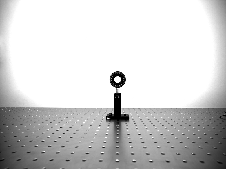
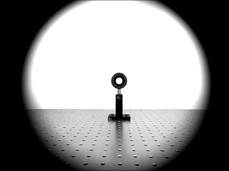
Figure 3: The vignetting effect is illustrated in the two images above, which were both captured using the same 4/3" format camera. a: Using a 12 mm focal length, 4/3" format lens produces a full image with slight dimming around the edges. This minor example of vignetting is due to the lens design which has decreased transmission at the edge of the lens. b: A 2/3" format lens at the same focal length produces a prominent dark ring around the photo edge.
| Recommended System Requirements | |
|---|---|
| Operating System | Windows® 7, 10, or 11 (64 Bit) |
| Processor (CPU)a |
≥3.0 GHz Intel Core (i5 or Newer) |
| Memory (RAM) | ≥8 GB |
| Hard Drive | ≥500 GB (SATA) Solid State Drive (SSD)b |
| Graphics Card | Dedicatedc Adapter with ≥256 MB RAM |
| Power Supply | ≥600 W |
| Motherboard | Integrated Intel USB 3.0 Controller or One Unused PCIe x1 Slot (for Item # USB3-PCIE) |
| Connectivity | USB or Internet Connectivity for Driver Installation |
Camera Interface
When using these scientific cameras, it is important to confirm that the computer system meets or exceeds the recommended requirements listed to the right; otherwise, dropped frames may result, particularly when streaming camera images directly to storage media.
Definitions
- Camera Frame Rate: The number of images per second generated by the camera. It is a function of camera model and user-selected settings.
- Effective Frame Rate: The number of images per second received by the host computer's camera software. This depends on the limits of the selected interface hardware (chipset), CPU performance, and other devices and software competing for the host computer resources.
- Maximum Bandwidth: The maximum rate (in bits/second or bytes/second) at which data can be reliably transferred over the interface from the camera to the host PC. The maximum bandwidth is a specified performance benchmark of the interface, under the assumption that the host PC is capable of receiving and handling data at that rate. An interface with a higher maximum bandwidth will typically support higher camera frame rates, but the choice of interface does not by itself increase the frame rate of the camera.
USB 3.0
USB 3.0 is a standard interface available on most new PCs, which means that typically no additional hardware is required, and therefore these cameras are not sold with any computer hardware. For users with PCs that do not have a USB 3.0 port, we offer a PCIe card. USB 3.0 supports a speed up to 320 MB/s and cable lengths up to 3 m, however maximum speeds can be impacted by the host PC's chipset. Support for multiple cameras is possible using multiple USB 3.0 ports on the PC or a USB 3.0 hub.
Scientific Camera Interface Summary
| Interface | USB 3.0 |
|---|---|
| Interface Image (Click to Enlarge) |  |
| Maximum Cable Length | 3 m |
| Maximum Bandwidtha | 320 MB/s |
| Support for Multiple Cameras | Via Multiple USB 3.0 Ports or Hub |
| Available Cameras | Zelux® 1.6 MP CMOS Kiralux® 1.3 MP CMOS Quantalux® 2.1 MP sCMOS Camera Kiralux 2.3 MP CMOS Cameras Kiralux 5 MP CMOS Cameras Kiralux 5 MP CMOS Polarization Camera Kiralux 8.9 MP CMOS Cameras Kiralux 12.3 MP CMOS Cameras |
Triggered Camera Operation
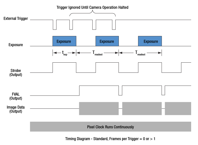
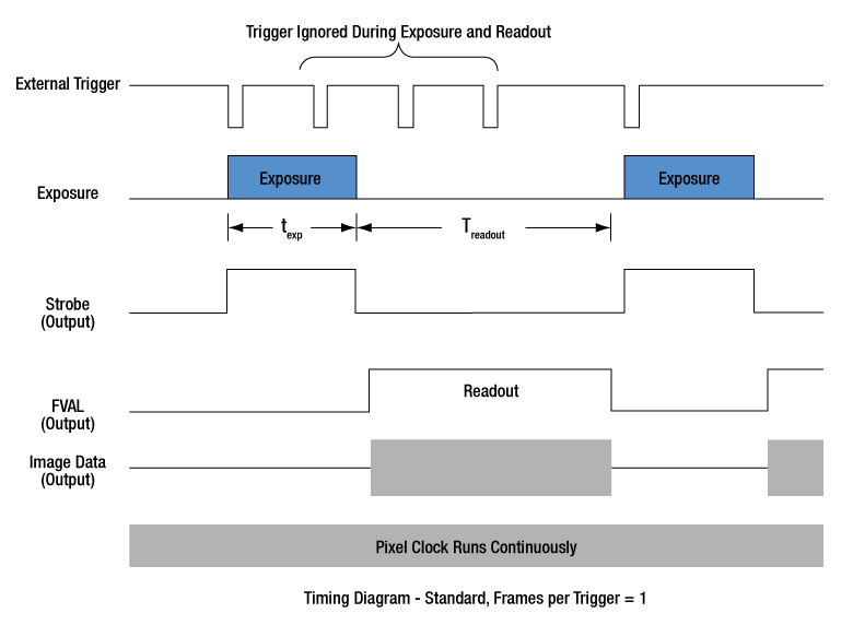
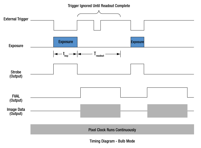
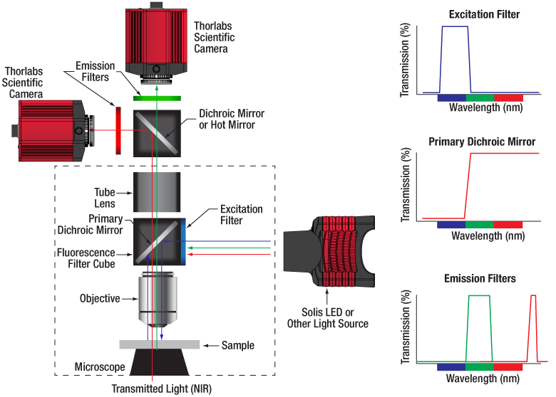
Our scientific cameras have three externally triggered operating modes: streaming overlapped exposure, asynchronous triggered acquisition, and bulb exposure driven by an externally generated trigger pulse. The trigger modes operate independently of the readout (e.g., 20 or 40 MHz; binning) settings as well as gain and offset. Figures 1 through 3 show the timing diagrams for these trigger modes, assuming an active low external TTL trigger. Please note that the Zelux® cameras do not have an FVAL Output; for diagrams specific to the Zelux cameras, click here.
Click to Enlarge
Figure 1: Streaming overlapped exposure mode. When the external trigger goes low, the exposure begins, and continues for the software-selected exposure time, followed by the readout. This sequence then repeats at the set time interval. Subsequent external triggers are ignored until the camera operation is halted.
Click to Enlarge
Figure 2: Asynchronous triggered acquisition mode. When the external trigger signal goes low, an exposure begins for the preset time, and then the exposure is read out of the camera. During the readout time, the external trigger is ignored. Once a single readout is complete, the camera will begin the next exposure only when the external trigger signal goes low.
Click to Enlarge
Figure 3: Bulb exposure mode. The exposure begins when the external trigger signal goes low and ends when the external trigger signal goes high. Trigger signals during camera readout are ignored.
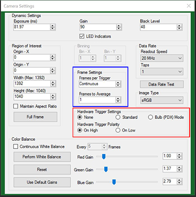
Figure 4: The ThorCam Camera Settings window. The red and blue highlighted regions indicate the trigger settings as described in the text.
External triggering enables these cameras to be easily integrated into systems that require the camera to be synchronized to external events. The Strobe Output goes high to indicate exposure; the strobe signal may be used in designing a system to synchronize external devices to the camera exposure. External triggering requires a connection to the auxiliary port of the camera. We offer the 8050-CAB1 auxiliary cable as an optional accessory. Two options are provided to "break out" individual signals. The TSI-IOBOB provides SMA connectors for each individual signal. Alternately, the TSI-IOBOB2 also provides the SMA connectors with the added functionality of a shield for Arduino boards that allows control of other peripheral equipment. More details on these three optional accessories are provided below.
Trigger settings are adjusted using the ThorCam software. Figure 4 shows the Camera Settings window, with the trigger settings highlighted with red and blue squares. Settings can be adjusted as follows:
- "HW Trigger" (Red Highlight) Set to "None": The camera will simply acquire the number of frames in the "Frames per Trigger" box when the capture button is pressed in ThorCam.
- "HW Trigger" Set to "Standard": There are Two Possible Scenarios:
- "Frames per Trigger" (Blue Highlight) Set to Zero or >1: The camera will operate in streaming overlapped exposure mode (Figure 1).
- "Frames per Trigger" Set to 1: Then the camera will operate in asynchronous triggered acquisition mode (Figure 2).
- "HW Trigger" Set to "Bulb (PDX) Mode": The camera will operate in bulb exposure mode, also known as Pulse Driven Exposure (PDX) mode (Figure 3).
In addition, the polarity of the trigger can be set to "On High" (exposure begins on the rising edge) or "On Low" (exposure begins on the falling edge) in the "HW Trigger Polarity" box (highlighted in red in Figure 4).
Equal Exposure Pulse (EEP) Mode
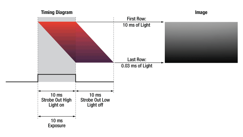
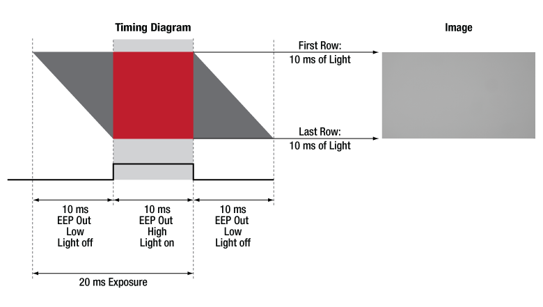
CMOS sensors often feature a rolling shutter, meaning that each row begins to acquire charge sequentially, rather than simultaneously as with the gloabal shutter on CCD sensors. If an external light source is triggered to turn on for the length of the exposure, this can lead to gradients across the image as different rows are illuminated for different lengths of time. The Equal Exposure Pulse (EEP) is an output signal available on our Quantalux® sCMOS camera's I/O connector. When selected in the ThorCam settings dialog, the strobe output signal is reconfigured to be active only after the CMOS sensor's rolling reset function has completed. The signal will remain active until the sensor's rolling readout function begins. This means that the signal is active only during the time when all of the sensor's pixels have been reset and are actively integrating. The resulting image will not show an exposure gradient typical of rolling reset sensors. Figure 5 shows an example of a strobe-driven exposure, where the strobe output is used to trigger an external light source; the resulting image shows a gradient as not all sensor rows are integrating charge for the same length of time when the light source is on. Figure 6 shows an example of an EEP exposure: the exposure time is lengthened, and the trigger output signal shifted to the time when all rows are integrating charge, yielding an image with equal illumination across the frame.
Please note that EEP will have no effect on images that are constantly illuminated. There are several conditions that must be met to use EEP mode; these are detailed in the User Guide.
Click to Enlarge
Figure 5: A timing example for an exposure using STROBE_OUT to trigger an external light source during exposure. A gradient is formed across the image since the sensor rows are not integrating charge for the same length of time the light source is on.
Click to Enlarge
Figure 6: A timing example for an exposure using EEP. The image is free of gradients, since the EEP signal triggers the light source only while all sensor rows are integrating charge.
Example: Camera Triggering Configuration using Thorlabs' Scientific Camera Accessories
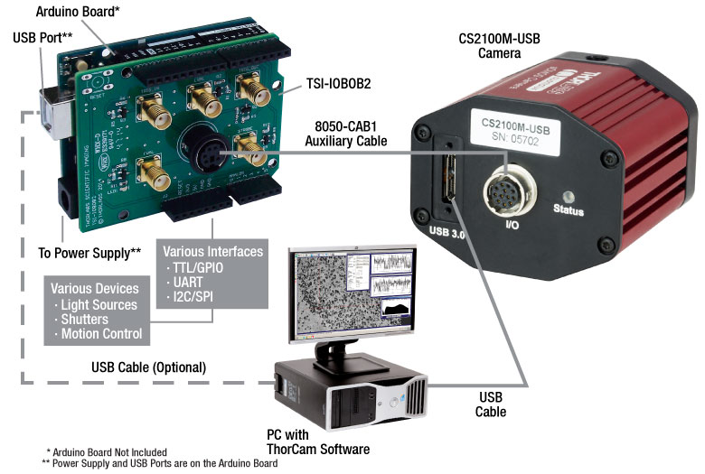
Figure 7: A schematic showing a system using the TSI-IOBOB2 to facilitate system integration and control.
As an example of how camera triggering can be integrated into system control is shown in Figure 7. In the schematic, the camera is connected to the TSI-IOBOB2 break-out board / shield for Arduino using a 8050-CAB1 cable. The pins on the shield can be used to deliver signals to simultaneously control other peripheral devices, such as light sources, shutters, or motion control devices. Once the control program is written to the Arduino board, the USB connection to the host PC can be removed, allowing for a stand-alone system control platform; alternately, the USB connection can be left in place to allow for two-way communication between the Arduino and the PC. Configuring the external trigger mode is done using ThorCam as described above.
Applications
Applications Overview
Thorlabs' Scientific-Grade Cameras are ideal for a variety of applications. The photo gallery below contains images acquired with our 1.4 MP CCD (previous generation), 4 MP CCD (previous generation), 8 MP CCD (previous generation), and fast frame rate CCD (previous generation) cameras.
To download some of these images as high-resolution, 16-bit TIFF files, please click here. It may be necessary to use an alternative image viewer to view the 16-bit files. We recommend ImageJ, which is a free download.
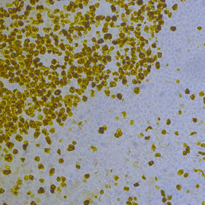
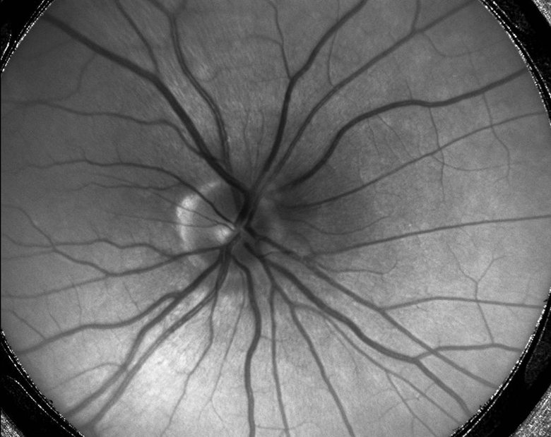
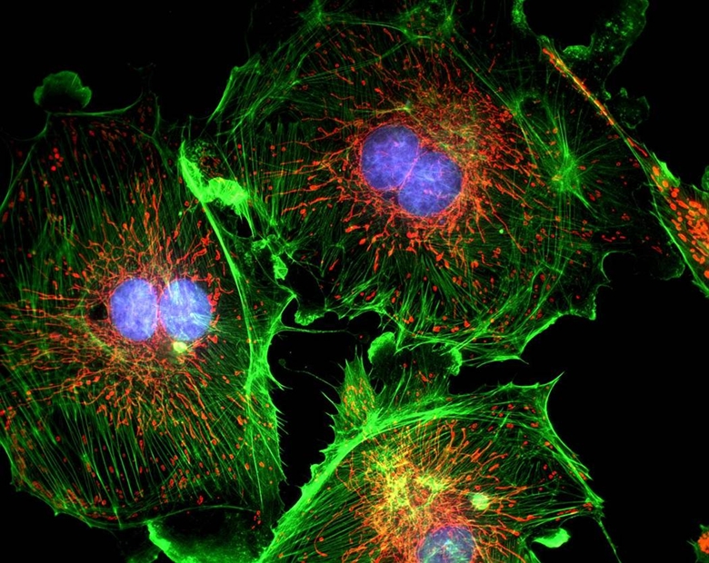
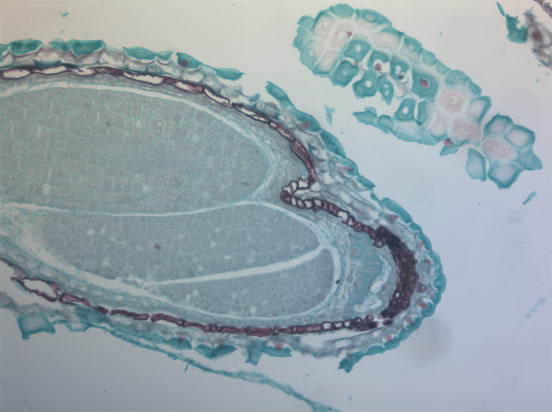
| Standard, Customized, or OEM Cameras and Software for a Range of Applications (Click Each Image for Details) | |||||
|---|---|---|---|---|---|
 |
 |
 |
 |
 |
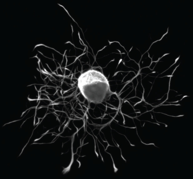 |
| Intracellular Dynamics | Brightfield Microscopy | Ophthalmology (NIR) | Fluorescence Microscopy | Multispectral Imaging | Neuroscience |
| Thorlabs' Scientific Cameras Recommended for Each Application Above | |||||
| Quantalux® 2.1 MP sCMOS | Kiralux® 1.3 MP CMOS Zelux™ 1.6 MP CMOS Kiralux 2.3 MP CMOS Kiralux 5 MP CMOS Kiralux 8.9 MP CMOS Kiralux 12.3 MP CMOS |
Kiralux 1.3 MP CMOS Kiralux 2.3 MP CMOS Kiralux 5 MP CMOS Kiralux 8.9 MP CMOS Kiralux 12.3 MP CMOS |
Quantalux 2.1 MP sCMOS Kiralux 2.3 MP CMOS Kiralux 5 MP CMOS Kiralux 8.9 MP CMOS Kiralux 12.3 MP CMOS |
Quantalux 2.1 MP sCMOS Kiralux 2.3 MP CMOS Kiralux 5 MP CMOS |
Quantalux 2.1 MP sCMOS Kiralux 2.3 MP CMOS Kiralux 5 MP CMOS Kiralux 8.9 MP CMOS Kiralux 12.3 MP CMOS |
Multispectral Imaging
The video to the right is an example of a multispectral image acquisition using a liquid crystal tunable filter (LCTF) in front of a monochrome camera. With a sample slide exposed to broadband light, the LCTF passes narrow bands of light that are transmitted from the sample. The monochromatic images are captured using a monochrome scientific camera, resulting in a datacube – a stack of spectrally separated two-dimensional images which can be used for quantitative analysis, such as finding ratios or thresholds and spectral unmixing.
In the example shown, a mature capsella bursa-pastoris embryo, also known as Shepherd's-Purse, is rapidly scanned across the 420 nm - 730 nm wavelength range using Thorlabs' previous-generation KURIOS-WB1 Liquid Crystal Tunable Filter. The images are captured using our legacy 1501M-GE Scientific Camera, which is connected, with the liquid crystal filter, to a Cerna® Series Microscope. The overall system magnification is 10X. The final stacked/recovered image is shown below.
Click to Enlarge
Final Stacked/Recovered Image
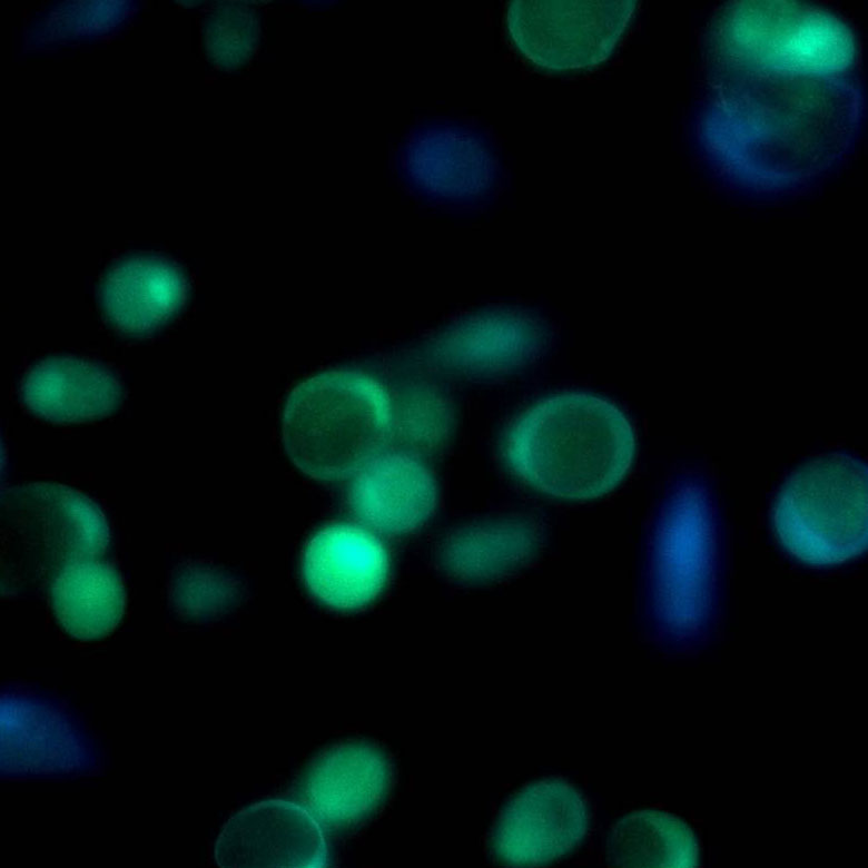
Thrombosis Studies
Thrombosis is the formation of a blood clot within a blood vessel that will impede the flow of blood in the circulatory system. The videos below are from experimental studies on the large-vessel thrombosis in Mice performed by Dr. Brian Cooley at the Medical College of Wisconsin. Three lasers (532 nm, 594 nm, and 650 nm) were expanded and then focused on a microsurgical field of an exposed surgical site in an anesthetized mouse. A custom, previous-generation 1.4 Megapixel Camera with integrated filter wheel was attached to a Leica Microscope to capture the low-light fluorescence emitted from the surgical site. See the videos below with their associated descriptions for further information.
Arterial Thrombosis
In the video above, a gentle 30-second electrolytic injury is generated on the surface of a carotid artery in an atherogenic mouse (ApoE-null on a high-fat, “Western” diet), using a 100-micron-diameter iron wire (creating a free-radical injury). The site (arrowhead) and the vessel are imaged by time-lapse fluorescence-capture, low-light camera over 60 minutes (timer is shown in upper left corner – hours:minutes:seconds). Platelets were labeled with a green fluorophore (rhodamine 6G) and anti-fibrin antibodies with a red fluorophore (Alexa-647) and injected prior to electrolytic injury to identify the development of platelets and fibrin in the developing thrombus. Flow is from left to right; the artery is approximately 500 microns in diameter (bar at lower right, 350 microns).
Venous Thrombosis
In the video above, a gentle 30-second electrolytic injury is generated on the surface of a murine femoral vein, using a 100-micron-diameter iron wire (creating a free-radical injury). The site (arrowhead) and the vessel are imaged by time-lapse fluorescence-capture, low-light camera over 60 minutes (timer is shown in upper left corner – hours:minutes:seconds). Platelets were labeled with a green fluorophore (rhodamine 6G) and anti-fibrin antibodies with a red fluorophore (Alexa-647) and injected prior to electrolytic injury to identify the development of platelets and fibrin in the developing thrombus. Flow is from left to right; the vein is approximately 500 microns in diameter (bar at lower right, 350 microns).
Reference: Cooley BC. In vivo fluorescence imaging of large-vessel thrombosis in mice. Arterioscler Thromb Vasc Biol 31, 1351-1356, 2011. All animal studies were done under protocols approved by the Medical College of Wisconsin Institutional Animal Care and Use Committee.
Click to Enlarge
Example Setup for Simultaneous NIR/DIC and Fluorescence Imaging
Live Dual-Channel Imaging
Many life science imaging experiments require a cell sample to be tested and imaged under varying experimental conditions over a significant period of time. One common technique to monitor complex cell dynamics in these experiments uses fluorophores to identify relevant cells within a sample, while simultaneously using NIR or differential interference contrast (DIC) microscopy to probe individual cells. Registering the two microscopy images to monitor changing conditions can be a difficult and frustrating task.
Live overlay imaging allows both images comprising the composite to be updated in real-time versus other methods that use a static image with a real-time overlay. Overlays with static images require frequent updates of the static image due to drift in the system or sample, or due to repositioning of the sample. Live overlay imaging removes that dependency by providing live streaming in both channels.
Using the ThorCam overlay plug-in with the two-way camera microscope mount, users can generate real-time two-channel composite images with live streaming updates from both camera channels, eliminating the need for frequent updates of a static overlay image. This live imaging method is ideal for applications such as calcium ratio imaging and electrophysiology.
Example Images
Simultaneous Fluorescence and DIC Imaging
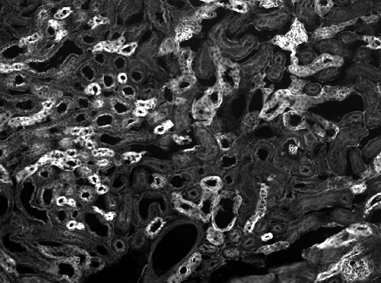
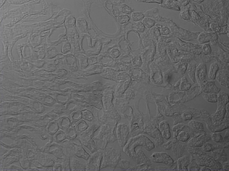
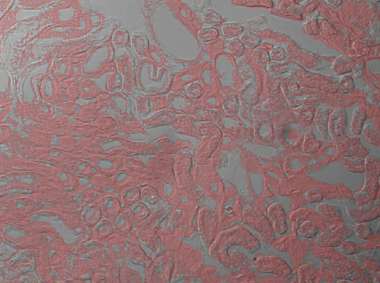
The image sequence below shows mouse kidney cells imaged using a dichroic filter to separate the fluorescence and DIC signals into different cameras. These images are then combined into a two-channel composite live image with false color fluorescence by the ThorCam overlay plug-in.
Click to Enlarge
Click to Enlarge
Click to Enlarge

Click to Enlarge
In the image above, the pipette is visible in the DIC image as two lines near the center of the frame.
Microaspiration Using a Micropipette
The image to the right shows a live, simultaneous overlay of fluorescence and DIC images. The experiment consists of a microaspiration technique using a micropipette to isolate a single neuron that expresses GFP. This neuron can then be used for PCR. This image was taken with our previous-generation 1.4 Megapixel Cameras and a two-camera mount and shows the live overlay of fluorescence and DIC from the ThorCam plug-in. Image courtesy of Ain Chung, in collaboration with Dr. Andre Fenton at NYU and Dr. Juan Marcos Alarcon at The Robert F. Furchgott Center for Neural and Behavioral Science, Department of Pathology, SUNY Downstate Medical Center.

Simultaneous NIR Dodt Contrast and Epi Fluorescence imaging
The image to the right shows a live, simultaneous overlay of fluorescence and near-infrared Dodt contrast images of a 50 µm brain section from a CX3CR1-GFP mouse, which has been immunostained for PECAM-1 with Alexa-687 to highlight vasculature. The Dodt contrast uses a quarter annulus and a diffuser to create a gradient of light across the sample that can reveal the structure of thick samples. The image was taken with our Scientific Cameras and a two-camera mount. Sample courtesy of Dr. Andrew Chojnacki, Department of Physiology and Pharmacology, Live Cell Imaging Facility, Snyder Institute for Chronic Diseases, University of Calgary.
| Posted Comments: | |
lin xue li
(posted 2021-04-15 17:20:04.027) I am appreciate that your company‘s presentation,however,If you can provide more details of the photovoltaic conversion of CCD(circuit,such as resistance value) and the gain coefficient of ADC,so much the better,thank you! YLohia
(posted 2021-04-21 11:01:15.0) Thank you for contacting Thorlabs. These parameters are model- and configuration-dependent. In other words, it depends on the camera model and sensor. Are you inquiring about a specific camera? If so, what's the part number? Additionally, could you please explain what you mean mean by "resistance value"? I had reached out to you at the time of your posting with these questions but never heard back. Adrian Alvarez
(posted 2020-12-17 17:28:41.323) I just wanted to say thanks for posting this helpful information on camera basics. YLohia
(posted 2020-12-18 11:46:54.0) Thank you very much for your feedback! We're always striving to provide our customers with relevant information about our products. |