Benchtop Photodiode Amplifier
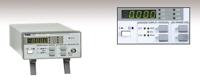
- Current Measurement Ranges: 100 nA to 10 mA
- Low Noise Operation
- Single Point Power Calibration
PDA200C
6 Current Ranges
Max. Resolution 10 pA

Please Wait
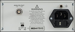
Click to Enlarge
The photodiode bias voltage, monitor control output (Analog Out), and grounding jack are located on the back panel of the PDA200C.
Compatible with all of Thorlabs' Mounted Photodiodes and Biased Photodetectors.
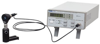
Click to Enlarge
PDA200C Benchtop Photodiode Amplifier Connected to an SM1-Threaded Mounted Photodiode Using a BNC Cable
Features
- Transimpedance Photocurrent Amplifier
- Extremely Low Noise Operation Over Entire Dynamic Range
- 5 Digit Display with up to 10 pA Resolution
- Supports Single Point Power Calibration
- Supports Both Photodiode Polarities (CG and AG)
- Adjustable Bias Voltage
- Offset Compensation for Input Amplifier and Photodiode Dark Current
- RoHS Compliant
The PDA200C Photodiode Amplifier is ideally suited for ultra-low-noise amplification of very small photodiode currents. It offers six current ranges from 100 nA to 10 mA full scale and provides a maximum display resolution of 10 pA. The unit supports cathode grounded (CG) and anode grounded (AG) photodiodes. This amplifier may be operated in either photovoltaic or photoconductive mode. The adjustable bias voltage provides improved linearity of the responsivity and increased frequency response. This photodiode amplifier is compatible with all of Thorlabs' mounted photodiodes and biased photodetectors. Our SM05-threaded mounted photodiodes feature a female SMA connector; to convert to BNC either an adapter cable or electrical adapter may be used.
With the updated PDA200C Series, our Photocurrent Amplifier is RoHS compliant. Additionally, the current measurement ranges were changed. The rest of the features are virtually the same as the former PDA200 Series.
Thorlabs recommends recalibrating these amplifiers every 24 months and offers a factory recalibration service. To order this service, scroll to the bottom of the page and select the CAL-CCS2.
| PDA200C Specifications | |
|---|---|
| Full Scale Current Measurement Ranges | 100 nA to 10 mA (in Decade Steps) |
| Maximum Resolution | 10 pA |
| Display Range | 0 to 10000 (CG) 0 to -10000 (AG) |
| Polarity of the Photodiode | Cathode Grounded (CG) Anode Grounded (AG) |
| Bias Voltage | 0 to -10 V (CG) 0 to +10 V (AG) |
| Photodiode Sensitivity (for Calibrated Power Display) | 0.05 to 2 A/W |
| Max. Photodiode Capacitance for Frequency Compensated Operation |
10 nF |
| Temperature Coefficient | <50 ppm/°C |
| Input Impedance | ~0 Ω (Virtual Ground) |
| Photo Current Monitor Output | |
| Output Voltage Range (Analog Output) | 0 to +10 V (CG) 0 to -10 V (AG) |
| Conversion Coefficient | 1 x 10³ to 1 x 10⁸ (Depending on Measurement Range) |
| Conversion Coefficient Accuracy | ±5% |
| Noise | ≤0.02% (RMS, Full Scale of Current Measurement Range) |
| Load Resistance | >10 kΩ |
| General Data | |
| Display | LED, 5 Digits |
| Connectors for Photodiode Input and Analog Output | BNC |
| Chassis Ground Connector | 4 mm Banana Jack |
| Line Voltage / Frequency |
100 V, 115 V, 230 V +15% -10% each / 50 to 60 Hz |
| Maximum Power Consumption | 10 VA |
| Mains Supply Overvoltage | Category II (Cat II) |
| Operating Temperature | 0 to +40 °C |
| Storage Temperature | -40 to +70 °C |
| Relative Humidity | Max. 80% Up to 31 °C, Decreasing to 50% at 40 °C |
| Pollution Degree (Indoor Use Only) | 2 |
| Operation Altitude | <2000 m |
| Warm-up Time for Rated Accuracy | 10 min |
| Weight | <3 kg |
| Dimensions without Operating Elements (W x H x D ) |
146 mm x 66 mm x 290 mm |
| Dimensions with Operating Elements (W x H x D ) |
146 mm x 77 mm x 320 mm |
| Measurement Range |
Resolution | Accuracy | Analog PD Current Output | |
|---|---|---|---|---|
| Conversion Coefficient | Bandwidtha | |||
| 10 mA | 1 µA | ± 0.05% f.s. | 1 x 10³ V/A ±5% | 500 kHz |
| 1 mA | 100 nA | ± 0.05% f.s. | 1 x 10⁴ V/A ±5% | 250 kHz |
| 100 µA | 10 nA | ± 0.05% f.s. | 1 x 10⁵ V/A ±5% | 70 kHz |
| 10 µA | 1 nA | ± 0.05% f.s. | 1 x 10⁶ V/A ±5% | 20 kHz |
| 1 µA | 100 pA | ± 0.05% f.s. | 1 x 10⁷ V/A ±5% | 5 kHz |
| 100 nA | 10 pA | ± 0.1% f.s. | 1 x 10⁸ V/A ±5% | 1 kHz |
Photodiode Input
BNC Female
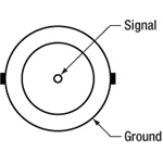
Input Range: 100 nA ... 10 mA
Analog Control Output
BNC Female

0 - ±10 V, Input Resistance should be ≥ 10 kΩ.
| PDA200C | Part |
|---|---|
| x | PDA200C Photodiode Amplifier |
| x | Operating Manual |
| x | Power Cord |
Insights into Best Lab Practices
Scroll down to read about a consideration when setting up lab equipment.
- Electrical Signals: AC vs. DC Coupling
Click here for more insights into lab practices and equipment.
Electrical Signals: AC vs. DC Coupling
When an instrument offers a choice between AC and DC coupled electrical inputs, it is not unusual for the DC coupling to be the better option for a modulated input signal.
Click to Enlarge
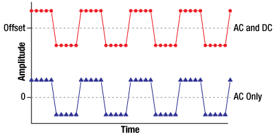
Figure 1: The DC offset of a signal is its average value. Since the blue curve (AC Only) has an average amplitude of zero, it has a zero DC offset. The red signal (AC and DC) is identical to the blue, except the red signal has a non-zero AC offset. A DC coupling would pass the red signal unchanged. An AC coupling would remove the DC offset and attenuate low-frequency components of the signal.
AC and DC Couplings
AC and DC couplings are interfaces between the input signal and the rest of the instrument's circuitry.
A DC coupling, which is called a direct coupling, is essentially a wire connected to the signal input. This conductive coupling transmits all of the signal's frequency components, the DC as well as the AC. The red curve in Figure 1 has a non-zero DC component.
In an AC coupling, the key feature is a capacitor placed in series with the signal input. The capacitor functions as a high-pass filter and is sometimes called a blocking capacitor. AC couplings strongly attenuate the DC and low-frequency signal components. This capacitive coupling is used to remove the DC offset from the input signal, so that only AC components are passed. The blue curve in Figure 1 has only AC frequency components.
Use the DC Coupled Input When Possible
There are many reasons to prefer the DC coupled input. Its low-frequency response is very good, it allows the DC component of the signal to be monitored along with the AC, and it does not cause signal distortion since it does not affect the frequency content of the signal.
Use of the DC coupled input is recommended unless the DC offset is large or the filtering provided by the AC coupled input is required. One problem with a large DC offset is that it can reduce the resolution of the instrument to unacceptably low levels. In extreme cases, DC offsets can cause clipping and saturation effects.
Note that using the DC coupled input does not guarantee a signal free of distortion. Distortion can occur due to other reasons, such as insufficient device bandwidth or impedance mismatch at the termination.
Click to Enlarge
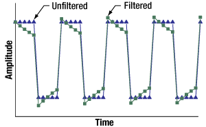
Figure 3: Some modulated signals, including the blue curve plotted above, have no DC component, but they do have non-negligible low-frequency components. When this signal is high-pass filtered by an AC coupling, the resulting signal is distorted. The green curve is one example of this.
Click to Enlarge
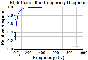
Figure 2: This frequency response magnitude plotted above models a capacitor-based high-pass filter. Its cutoff frequency (Fc) is 35 Hz, and it was used to filter the signal plotted in Figure 3. That signal has a repetition rate of 200 Hz.
Reasons to Use the AC Coupled Input
By rejecting the signal's DC component, AC coupling can reduce the total amplitude of the signal. This can increase the measurement resolution provided by the instrument, as well as overcome saturation and clipping problems. AC coupling provides good results when information is carried by high frequency signal components and low frequency components are not of interest. AC coupling can also be preferred when the application does not tolerate DC frequency signal components, as is the case for some telecommunications applications.
When Using the AC Coupled Input
If AC coupling is used, it is important to keep in mind that this coupling acts as a high pass filter and affects the frequency content of the signal.
As illustrated by Figure 2, this coupling does not just remove the DC offset, it can also attenuate low frequency components that may be of interest. Due to this, AC coupling can result in signal distortion. To illustrate the effects of high-pass filtering, Figure 3 plots a binary signal, with 200 Hz repetition rate, before and after it is filtered by the high-pass filter with 35 Hz cutoff frequency (Fc).
AC-coupled, digital telecommunications signals mitigate this problem by ensuring the signals are DC balanced, so that they have no DC offset. If the signals were not DC balanced, a series of ones could cause a sustained high signal level. This would introduce a non-zero DC level that would cause the signal to be affected by the capacitive filtering. The result could be bit errors due to high states being incorrectly read as low states.
Date of Last Edit: Dec. 4, 2019
| Posted Comments: | |
Stephen Keen
(posted 2023-10-19 09:06:37.853) Hi
We have two of these amps and they work well. As mentioned in other threads the biggest issue is with indication of which gain range your on.
We have an automation task that ideally we could electronically switch between gain ranges. Is there anyway of achieving this with the current configuration (at customer risk mods).
I would recommend this as a future feature
regards dpossin
(posted 2023-11-03 09:48:33.0) Dear Stephen,
Thank you for your feedback. I would consider that as a special as well. I forward this to our presales team and they will get in contact with you regarding lead time and price ASAP. Brad Frazer
(posted 2023-06-01 16:03:55.707) Can the PDA200C be used with an external bias (say ~50V) to enable use with a SiPM device operating in current mode? dpossin
(posted 2023-06-07 10:03:32.0) Dear Brad,
Thank you for your feedback! The PDA200C unfortunatey can just provide a bias voltage up to 10V. Chi Wang
(posted 2021-08-19 00:11:35.29) Hello, we are planning to build a fiber light power monitor. The power range in fiber we want to monitor is between 1nW to 1mW. We plan to use DET01CFC to detect light and then out put to a PDA200C. Then to readout power directly on PDA200C or connect it onto a PDA200C. Is it possible to use these two parts to accomplish this function? Looking forward to your reply! soswald
(posted 2021-08-23 06:00:34.0) Dear Chi Wang,
thank you for your feedback. In principle the DET01CFC + PDA200C can be used to measure such optical powers.
I have reached out to you directly to discuss your application in more detail and look at bandwidth and wavelength requirements. SEUNGHO LEE
(posted 2021-07-10 10:20:56.427) Hello,
I am thinking that PDA200C will be used together with DET08C which can receive 5GHz photo-signal. Does this PDA200C amplify the fast signal? I am asking this question because I saw, in the section of High-speed Free-space detectors, the photo that inspires DET025A(bandwidth 2GHz) is used with PDA200C.
Thanks ,
SHLee soswald
(posted 2021-07-13 03:30:34.0) Dear Seungho Lee,
thank you for your feedback. The PDA200C can be used to amplify the signal from detectors like DET025A.
Unfortunately the PDA200C does not reach a bandwidth of 2 or even 5 GHz. The maximum small signal bandwidth of the PDA200C is 500 kHz, although this depends on the measurement range.
Please see Section 5.1 of the manual for further information.
I have contacted you directly to discuss your application in more detail. Peter Kreuser
(posted 2021-06-28 13:18:12.053) Hello, how do I find the best amplifier settings for my specific detector? soswald
(posted 2021-07-05 06:30:15.0) Dear Peter,
thank you for your feedback. The best amplification setting will be highly dependent on the responsitivity of your photodiode and the optical power incident on the detector.
We recommend to start at the minimum amplification setting (10 mA measurement range) when connecting a photodiode for the first time and then switching through higher amplification settings until the current is displayed with sufficient resolution on the display.
Please see Section 3.2.1 of the manual (https://www.thorlabs.de/drawings/6973049f683fe8db-94298CF0-9F25-D151-C6C4E3066BFB71B2/PDA200C-Manual.pdf) for further information on this topic. melanie holmes
(posted 2020-02-06 10:51:48.923) Hi,
We have a strong 50 Hz signal when using this device on its two highest gain settings. Is that expected ?
The signals we are measuring are modulated at between 100 Hz and 760 Hz so your mains hum filter is not suitable.
Can you please suggest a solution ?
Thanks ! MKiess
(posted 2020-02-06 10:38:10.0) This is a response from Michael at Thorlabs. Thank you very much for your inquiry. I have contacted you directly to discuss your complete measurement setup and possible reasons for this signal. Raymond.Chan
(posted 2019-01-09 09:24:39.903) Hi,
Can you customize the pda200c so that it could measure current up to 100ma?
We could accept customization charges.
Else could you advice how we can modify it so that it could display up 100ma? wskopalik
(posted 2019-01-11 03:21:08.0) This is a response from Wolfgang at Thorlabs. Thank you very much for your feedback!
I will contact you directly to see if we can offer a suitable customization. As the PDA200C is designed for photodiodes which usually don't provide that much current, I would like to make sure that it is really suitable for your application. eli.quinicot
(posted 2018-03-08 06:06:07.61) Hi I'd like to know if this could be used for measuring low currents from a solar cell.
This product would give me an output of voltage right? Thanks swick
(posted 2018-03-16 04:08:34.0) This is a response from Sebastian at Thorlabs. Thank you for the inquiry. The measurement principle in PDA200C is based on input resistance to be 0 Ohm. That means the connected sensor needs to deliver only electrical current and no voltage. For photodiodes this is the case but not necessarily for solar cells. melanie
(posted 2015-02-04 18:21:47.36) Hi,
Thanks for answer about source impedance. Does that mean we should not connect to a DAQ board using a 50 Ohm BNC cable ? If so, what should we use instead ? shallwig
(posted 2015-03-05 06:58:11.0) This is a response from Stefan at Thorlabs. Thank you again for your further questions. You are correct, you should not connect the PDA200C to a 50 Ohm BNC cable. If you connect a resistance with less than 10kOhm the internal amplifier is not able to provide the output voltage of 10V. You will get an output error. To use the PDA200C together with your DAQ board you can use a voltage follower circuit. This voltage follower circuit must have an input resistance of 10 kOhm to match the photodiode amplifier requirement, and an output resistance of 50 Ohms to work well with your DAQ board. We have contacted you directly to discuss your application in more detail. user
(posted 2015-01-31 15:55:52.48) Please can you tell me the source impedance of the analog output ? I need this number to choose optimum settings for my DAQ board. Thank you. shallwig
(posted 2015-02-03 07:31:22.0) This is a response from Stefan at Thorlabs. Thank you very much for your inquiry. The source impedance of the analog output for this device is 10kOhm. robertmeissner
(posted 2014-11-17 15:46:20.173) We use a PDA200C. When I turn it on (no Diode connected), it does nothing. I checked fuses (everything alright), tried several cables and plugs, so far to no end. We are using 230V and I specificially changed the fused to 230V.
So far, nobody seems to have used it (as the fuse holder was placed to 115V and we only have 230V). Is there any hidden Switch or so that I have to press (of course I tried the button on the front. shallwig
(posted 2014-11-18 02:32:32.0) This is a response from Stefan at Thorlabs. Thank you very much for your inquiry. I am sorry for the problems you face with our photodiode amplifier. There is no hidden switch which is supposed to be used to get the device work. Only the line voltage has to be set correctly before using the device first time. I will contact you directly for further troubleshooting. melanie
(posted 2014-08-14 15:53:13.967) This feedback is concerning the Benchtop Photodiode Amplifier.
Yes it will be useful.
However, if the current range could be set remotely, eg over GPIB or USB, then it would be amazing.
Please consider this upgrade. I want to use it for automated measurements that are in several stages, between stages I will need to change range and it would be easier to do via computer comms than manually. shallwig
(posted 2014-08-26 08:16:17.0) This is a response from Stefan at Thorlabs. Thank you very much for your feedback about the PDA200C. The devices of this series are apart from the display analog devices and do not support digital interfaces. Reason for that is the low processing power of the devices. At the moment it is not planned to upgrade them as this would lead to a complete redesign of the device but I forwarded your ideas to our engineers. I will contact you directly to discuss your application in detail. tschalk
(posted 2012-12-06 03:17:00.0) This is a response from Thomas at Thorlabs. Thank you very much for your inquiry. The PDA200C is immediately ready to use after turning on the device. It makes no difference if you connect the photodiode before or after turning on the amplifier and it is independent of using a bias voltage. If you have to turn the device off and on again for getting a measurement indicates that something is wrong with the connection or with the device itself. I will contact you directly to discuss this issue. Best Regards, Thomas sal.leap
(posted 2012-12-03 13:47:32.817) I have a few PDA 200C that I have to recycle the power to the unit to get power readings from a FDG-50 large area detector. I have an external power source aimed at the LAD but the PDA 200C does not display any power. But when I recycle the power to the amplifier it shows detected power.
Regards,
Sal (Process Engineer, Molex) tcohen
(posted 2012-05-23 11:28:00.0) Response from Tim at Thorlabs: Thank you for sharing your ideas! Because these changes cannot be directly integrated into the current model, these suggestions would involve a full redesign of the PDA200C. Currently, our engineers are fully engaged in the development of new products, but based on your suggestions we have opened a discussion so that we may start the development of this as a future project and offer these features in a PDA200C successor. acable
(posted 2012-05-22 10:00:54.0) It would be great to have an indicator that tells the user what gain step the PDA200C is set to, when making a complex series of measurements that require changes in gain this feature would be really welcome. The current design uses 3 LEDs with 2 steps per LED which is difficult in a real world application to track.
Smaller point, a number of your SI photodiodes are spec'd at 20V bias but the PDA200 only goes to 10V, i am assuming you would spec your diodes at their optimal bias hence i feel that i am not getting the best possible performance from my setup. Please consider increasing the bias to 20 V.
Sincerely grateful for your attention! tcohen
(posted 2012-05-15 10:17:00.0) Response from Tim at Thorlabs: Thank you for contacting us. The “Err06” error message indicates a malfunction of the PCB in the device and we will need to take it in to repair. We will contact you with information and instructions. jjwang
(posted 2012-05-15 13:50:11.0) Dear Sir/Madam,
We had a problem with PDA200C and it reports "Err06". Would you please provide us the solution to sort out this problem.
Best Regards,
Dr Jing Jing Wang
Centre for Research on Adaptive Nanostructures and Nanodevices
Trinity College Dublin
Dublin 2
Ireland
Telephone: 0035318964633 (Office)
0035318964617 (Photonics Laboratory)
Email: jjwang@tcd.ie julien
(posted 2010-04-22 09:44:53.0) A response from Julien at Thorlabs: "Err06" is displayed on the unit when an electronic problem occurs on the PCB leading to a malfunction of the PDA200C. The unit thus needs to be sent to us for repair. For errors not listed, the manual recommend to contact directly tech support, since those errors cannot be fixed by the user. I will contact you directly to initiate the return procedure. davepatterson99
(posted 2010-04-21 12:22:52.0) I have a PDA 200 C. When I turn it on (no diode connected) it says "Err06". Your manual says nothing about "Err06". This is terrible! The unit is quite new (about one year). Please send me the real manual? |
Transimpedance Amplifier Selection Guide
| Representative Photoa |
Item # | Zero Offset |
PD Bias Voltage |
Bandwidth (3 dB) |
Transimpedance Gain |
Max Input Current |
Max Output Voltage |
Max PD Capacitanceb |
Power Supply |
Mass | Dimensions |
|---|---|---|---|---|---|---|---|---|---|---|---|
| Fixed Gain, Compact | |||||||||||
 |
AMP110 |  |
- | 1 kHz | 107 V/A | ±200 nA | ±2 V | 10 nF | USB, 5 V @ 2 A |
80 g | 97 mm x 32 mm x 25.4 mm |
| AMP120 |  |
- | 100 kHz | 105 V/A | ±20 µA | ±2 V | 10 nF | ||||
| AMP130 |  |
- | 100 kHz | 103 V/A | ±2 mA | ±2 V | 10 nF | ||||
| AMP140 | - |  |
10 MHz | 104 V/A | ±350 µA | ±3.5 Vc | 200 pF | 96 mm x 32 mm x 25.4 mm | |||
| Switchable Gain, Compact | |||||||||||
 |
AMP100 |  |
- | 1 kHz | 106 V/A | ±2 µA | ±2 V | 10 nF | USB, 5 V @ 2 A |
80 g | 97 mm x 32 mm x 25.4 mm |
| 107 V/A | ±200 nA | ||||||||||
| 108 V/A | ±20 nA | ||||||||||
| AMP102 |  |
- | 100 kHz | 103 V/A | ±2 mA | ±2 V | 10 nF | ||||
| 104 V/A | ±200 µA | ||||||||||
| 105 V/A | ±20 µA | ||||||||||
| Switchable Gain, Benchtop with 5-Digit LED Display | |||||||||||
 |
PDA200C |  |
 |
1 kHz | 108 V/A | +100 nA | ±10 Vd | 10 nF | 100 V, 115 V, or 230 V (50/60 Hz) |
<3 kg | 320 mm x 146 mm x 77 mm |
| 5 kHz | 107 V/A | +1 µA | |||||||||
| 20 kHz | 106 V/A | +10 µA | |||||||||
| 70 kHz | 105 V/A | +100 µA | |||||||||
| 250 kHz | 104 V/A | +1 mA | |||||||||
| 500 kHz | 103 V/A | +10 mA | |||||||||

| Key Specificationsa | |
|---|---|
| Full Scale Current Measurement Ranges | 100 nA to 10 mA (in Decade Steps) |
| Maximum Resolution | 10 pA |
| Bias Voltage | 0 to -10 V (CG) 0 to +10 V (AG) |
| Noise | ≤0.02%b |
| Analog PD Current Output Bandwidth | DC to 500 kHzc |
| Analog PD Current Output Conversion Coefficient | 103 V/A to 108 V/Ac |
- Transimpedance Photocurrent Amplifier
- Extremely Low Noise Operation Over Entire Dynamic Range
- Supports Single Point Power Calibration
Thorlabs' PDA200C Photodiode Amplifier is ideally suited for ultra-low-noise amplification of very small photodiode currents. It offers six current ranges from 100 nA to 10 mA full scale and provides a maximum display resolution of 10 pA. The unit supports cathode grounded (CG) and anode grounded (AG) photodiodes. This amplifier may be operated in either photovoltaic or photoconductive mode. The adjustable bias voltage provides improved linearity of the responsivity and increased frequency response. This photodiode amplifier is compatible with all of Thorlabs' mounted photodiodes and biased photodetectors.

Thorlabs offers a recalibration service for the PDA200C Benchtop Photodiode Amplifier. To ensure accurate measurements, we recommend recalibrating this device every 24 months.
Requesting a Calibration
Thorlabs provides two options for requesting a calibration:
- Complete the Returns Material Authorization (RMA) form. When completing the RMA form, please enter your name, contact information, the Part #, and the Serial # of the item being returned for calibration; in the Reason for Return field, select "I would like an item to be calibrated." All other fields are optional. Once the form has been submitted, a member of our RMA team will reach out to provide an RMA Number, return instructions, and to verify billing and payment information.
- Enter the Part # and Serial # of the item that requires recalbration below and then Add to Cart. A member of our RMA team will reach out to coordinate return of the item for calibration. Should you have other items in your cart, note that the calibration request will be split off from your order for RMA processing.
Please Note: To ensure your item being returned for calibration is routed appropriately once it arrives at our facility, please do not ship it prior to being provided an RMA Number and return instructions by a member of our team.
 Products Home




 Zoom
Zoom Benchtop Transimpedance Amplifier