 Products Home / Detectors / Transimpedance & Voltage Amplifiers / Voltage Amplifiers for Photodetectors
Voltage Amplifiers for Photodetectors
- Fixed or Adjustable Voltage Gain up to 1000 V/V
- Bandwidth: DC to 100 kHz
- Rise/Fall Time: <3 µs
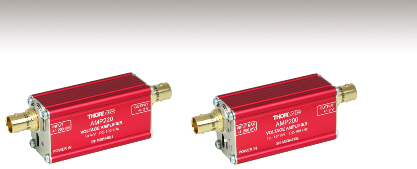
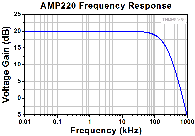
AMP220
Gain: 10 V/V
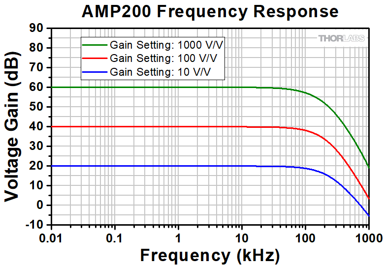
AMP200
Switchable Gain:
10, 100, or 1000 V/V


Please Wait

Click to Enlarge
The AMP200 Amplifier's gain selector switch is located on the input BNC connector end, alongside the power LED and USB connector.
Click to Enlarge
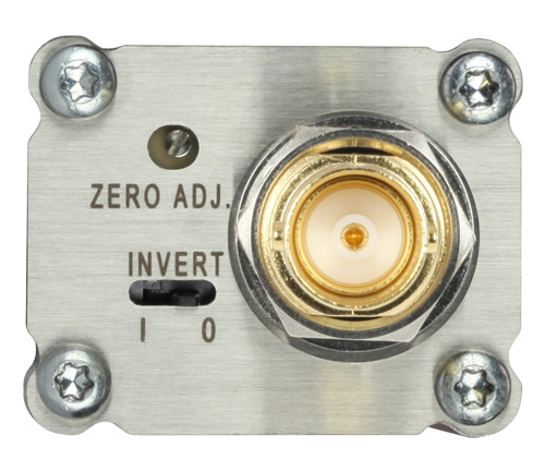
The voltage offset adjuster and polarity switch are located on the output BNC connector end.
Features
- 100 kHz Bandwidth
- <3 µs Rise/Fall Time
- Fixed and Switchable Gain Models
- Max Input Voltages:
- AMP220: ±200 mV
- AMP210: ±2 mV
- AMP200: ±200 mV, ±20 mV, or ±2 mV (Differs with Selected Gain)
- Adjustable Voltage Offset for Dark Current Compensation
- Compact, In-Line Design for Use Between Two BNC Cables
- DS5 USB Power Supply and 1.5 m Long Micro-B USB Cable Included
Thorlabs' AMP200 Series of Voltage Amplifiers are designed to amplify the output signal from low-output-voltage devices such as thermopile power detectors, photoconductive detectors, or pyroelectric energy detectors. The offset caused by the dark current of a connected photodetector can be compensated for using the Zero Adjust screw on the output end of the amplifier (see image to the right). A switch allows the output signal's sign to be set based on the connected photodetector's polarity (Invert: 1/On or 0/Off).
Each voltage amplifier has an in-line box design with two female BNC connectors and is intended to be used between two BNC cables. These amplifiers are powered through a Micro-B USB port using the included 5 V, 2 A power supply or any other available USB port. An LED next to the USB connector indicates active power supply. The internal electronics of the amplifier regulate the power to the amplification circuitry, isolating the device's performance from electrical noise that may be inherent to the power source.
| Specifications | ||||
|---|---|---|---|---|
| Item # | AMP220 | AMP210 | AMP200 | |
| Voltage Gain | 10 V/V (20 dB) | 1000 V/V (60 dB) | Switchable: 10 V/V (20 dB), 100 V/V (40 dB), or 1000 V/V (60 dB) |
|
| Bandwidth (3 dB, Rin: 50 Ω, Cin: 100 pF)a | DC to 100 kHz | |||
| Rise/Fall Time (10% to 90%) | <3 µs | |||
| Input Voltage Limitsb | ±200 mV | ±2 mV | ±200 mV @ 10 V/V ±20 mV @ 100 V/V ±2 mV @ 1000 V/V |
|
| Input Impedance | 1 MΩ | |||
| Input Noise Densitya | 7 nV/Hz1/2 | 2.5 nV/Hz1/2 | 7 nV/Hz1/2 @ 10 V/V 3.5 nV/Hz1/2 @ 100 V/V 2.5 nV/Hz1/2 @ 1000 V/V |
|
| Quiescent Current | 45 mA | |||
| Output Voltage Range | 50 Ω Load | ±1.0 V | ||
| Hi-Z Load | ±2.0 V | |||
| Output Voltage Offset Range | ±2 mV | ±200 mV | ±2 mV @ 10 V/V ±20 mV @ 100 V/V ±200 mV @ 1000 V/V |
|
| Output Impedance | 50 Ω | |||
| Included Power Supply | DS5 | |||
| Power Supply Voltage | 5 V | |||
| Power Supply Current | 2 A | |||
| Included USB Cable | Micro-B, 1.5 m Long | |||
| Dimensions (L x W x H) | 96.7 mm x 31.8 mm x 25.4 mm (3.81" x 1.25" x 1.00") |
|||
| Mass (Weight) | 80 g (2.8 oz) | |||
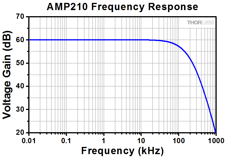
The graphs below represent calculated data using an input source with 50 Ω impedance and 100 pF capacitance.
Input Voltage Connector
BNC Female
1 MΩ Input Impedance
Output Voltage Connector
BNC Female
50 Ω Recommended Termination
Power Supply Connector
Micro-B USB
Photodiode Tutorial
Theory of Operation
A junction photodiode is an intrinsic device that behaves similarly to an ordinary signal diode, but it generates a photocurrent when light is absorbed in the depleted region of the junction semiconductor. A photodiode is a fast, highly linear device that exhibits high quantum efficiency and may be used in a variety of different applications.
It is necessary to be able to correctly determine the level of the output current to expect and the responsivity based upon the incident light. Depicted in Figure 1 is a junction photodiode model with basic discrete components to help visualize the main characteristics and gain a better understanding of the operation of Thorlabs' photodiodes.
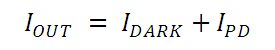
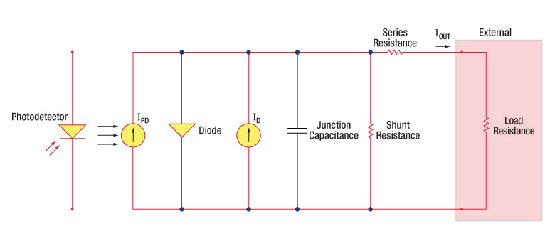
Figure 1: Photodiode Model
Photodiode Terminology
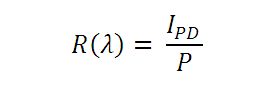
Responsivity
The responsivity of a photodiode can be defined as a ratio of generated photocurrent (IPD) to the incident light power (P) at a given wavelength:
Modes of Operation (Photoconductive vs. Photovoltaic)
A photodiode can be operated in one of two modes: photoconductive (reverse bias) or photovoltaic (zero-bias). Mode selection depends upon the application's speed requirements and the amount of tolerable dark current (leakage current).
Photoconductive
In photoconductive mode, an external reverse bias is applied, which is the basis for our DET series detectors. The current measured through the circuit indicates illumination of the device; the measured output current is linearly proportional to the input optical power. Applying a reverse bias increases the width of the depletion junction producing an increased responsivity with a decrease in junction capacitance and produces a very linear response. Operating under these conditions does tend to produce a larger dark current, but this can be limited based upon the photodiode material. (Note: Our DET detectors are reverse biased and cannot be operated under a forward bias.)
Photovoltaic
In photovoltaic mode the photodiode is zero biased. The flow of current out of the device is restricted and a voltage builds up. This mode of operation exploits the photovoltaic effect, which is the basis for solar cells. The amount of dark current is kept at a minimum when operating in photovoltaic mode.
Dark Current
Dark current is leakage current that flows when a bias voltage is applied to a photodiode. When operating in a photoconductive mode, there tends to be a higher dark current that varies directly with temperature. Dark current approximately doubles for every 10 °C increase in temperature, and shunt resistance tends to double for every 6 °C rise. Of course, applying a higher bias will decrease the junction capacitance but will increase the amount of dark current present.
The dark current present is also affected by the photodiode material and the size of the active area. Silicon devices generally produce low dark current compared to germanium devices which have high dark currents. The table below lists several photodiode materials and their relative dark currents, speeds, sensitivity, and costs.
| Material | Dark Current | Speed | Spectral Range | Cost |
|---|---|---|---|---|
| Silicon (Si) | Low | High Speed | Visible to NIR | Low |
| Germanium (Ge) | High | Low Speed | NIR | Low |
| Gallium Phosphide (GaP) | Low | High Speed | UV to Visible | Moderate |
| Indium Gallium Arsenide (InGaAs) | Low | High Speed | NIR | Moderate |
| Indium Arsenide Antimonide (InAsSb) | High | Low Speed | NIR to MIR | High |
| Extended Range Indium Gallium Arsenide (InGaAs) | High | High Speed | NIR | High |
| Mercury Cadmium Telluride (MCT, HgCdTe) | High | Low Speed | NIR to MIR | High |
Junction Capacitance
Junction capacitance (Cj) is an important property of a photodiode as this can have a profound impact on the photodiode's bandwidth and response. It should be noted that larger diode areas encompass a greater junction volume with increased charge capacity. In a reverse bias application, the depletion width of the junction is increased, thus effectively reducing the junction capacitance and increasing the response speed.
Bandwidth and Response
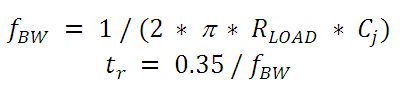
A load resistor will react with the photodetector junction capacitance to limit the bandwidth. For best frequency response, a 50 Ω terminator should be used in conjunction with a 50 Ω coaxial cable. The bandwidth (fBW) and the rise time response (tr) can be approximated using the junction capacitance (Cj) and the load resistance (RLOAD):
Noise Equivalent Power
The noise equivalent power (NEP) is the input signal power that results in a signal-to-noise ratio (SNR) of 1 in a 1 Hz output bandwidth. This is useful, as the NEP determines the ability of the detector to detect low level light. In general, the NEP increases with the active area of the detector and is given by the following equation:
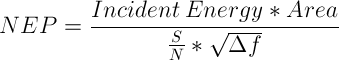
Here, S/N is the Signal to Noise Ratio, Δf is the Noise Bandwidth, and Incident Energy has units of W/cm2. For more information on NEP, please see Thorlabs' Noise Equivalent Power White Paper.
Terminating Resistance
A load resistance is used to convert the generated photocurrent into a voltage (VOUT) for viewing on an oscilloscope:
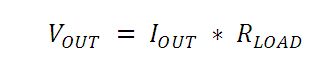
Depending on the type of the photodiode, load resistance can affect the response speed. For maximum bandwidth, we recommend using a 50 Ω coaxial cable with a 50 Ω terminating resistor at the opposite end of the cable. This will minimize ringing by matching the cable with its characteristic impedance. If bandwidth is not important, you may increase the amount of voltage for a given light level by increasing RLOAD. In an unmatched termination, the length of the coaxial cable can have a profound impact on the response, so it is recommended to keep the cable as short as possible.
Shunt Resistance
Shunt resistance represents the resistance of the zero-biased photodiode junction. An ideal photodiode will have an infinite shunt resistance, but actual values may range from the order of ten Ω to thousands of MΩ and is dependent on the photodiode material. For example, and InGaAs detector has a shunt resistance on the order of 10 MΩ while a Ge detector is in the kΩ range. This can significantly impact the noise current on the photodiode. For most applications, however, the high resistance produces little effect and can be ignored.
Series Resistance
Series resistance is the resistance of the semiconductor material, and this low resistance can generally be ignored. The series resistance arises from the contacts and the wire bonds of the photodiode and is used to mainly determine the linearity of the photodiode under zero bias conditions.
Common Operating Circuits
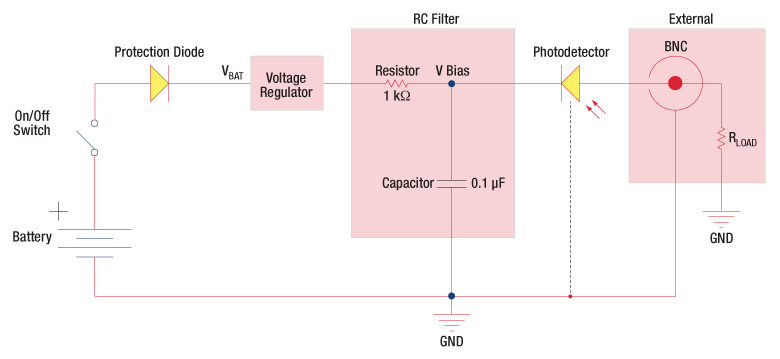
Figure 2: Reverse-Biased Circuit (DET Series Detectors)
The DET series detectors are modeled with the circuit depicted above. The detector is reverse biased to produce a linear response to the applied input light. The amount of photocurrent generated is based upon the incident light and wavelength and can be viewed on an oscilloscope by attaching a load resistance on the output. The function of the RC filter is to filter any high-frequency noise from the input supply that may contribute to a noisy output.
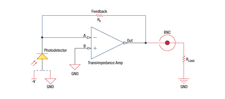
Figure 3: Amplified Detector Circuit
One can also use a photodetector with an amplifier for the purpose of achieving high gain. The user can choose whether to operate in Photovoltaic of Photoconductive modes. There are a few benefits of choosing this active circuit:
- Photovoltaic mode: The circuit is held at zero volts across the photodiode, since point A is held at the same potential as point B by the operational amplifier. This eliminates the possibility of dark current.
- Photoconductive mode: The photodiode is reversed biased, thus improving the bandwidth while lowering the junction capacitance. The gain of the detector is dependent on the feedback element (Rf). The bandwidth of the detector can be calculated using the following:
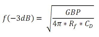
where GBP is the amplifier gain bandwidth product and CD is the sum of the junction capacitance and amplifier capacitance.
Effects of Chopping Frequency
The photoconductor signal will remain constant up to the time constant response limit. Many detectors, including PbS, PbSe, HgCdTe (MCT), and InAsSb, have a typical 1/f noise spectrum (i.e., the noise decreases as chopping frequency increases), which has a profound impact on the time constant at lower frequencies.
The detector will exhibit lower responsivity at lower chopping frequencies. Frequency response and detectivity are maximized for
![]()

Insights into Best Lab Practices
Scroll down to read about a consideration when setting up lab equipment.
- Electrical Signals: AC vs. DC Coupling
Click here for more insights into lab practices and equipment.
Electrical Signals: AC vs. DC Coupling
When an instrument offers a choice between AC and DC coupled electrical inputs, it is not unusual for the DC coupling to be the better option for a modulated input signal.
Click to Enlarge
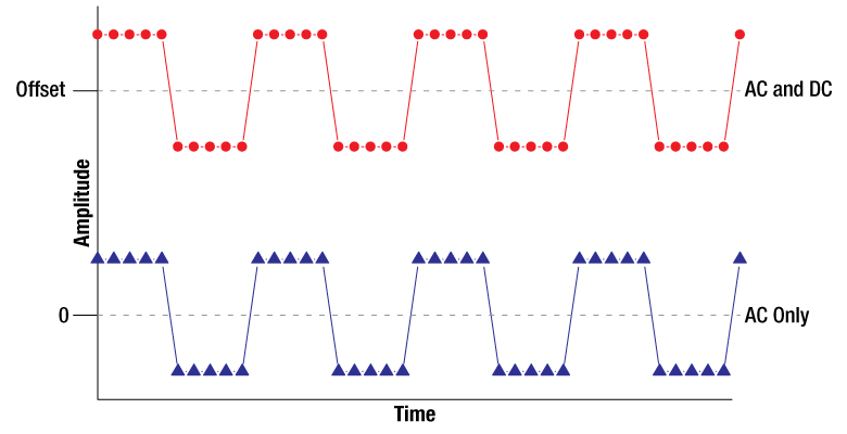
Figure 1: The DC offset of a signal is its average value. Since the blue curve (AC Only) has an average amplitude of zero, it has a zero DC offset. The red signal (AC and DC) is identical to the blue, except the red signal has a non-zero AC offset. A DC coupling would pass the red signal unchanged. An AC coupling would remove the DC offset and attenuate low-frequency components of the signal.
AC and DC Couplings
AC and DC couplings are interfaces between the input signal and the rest of the instrument's circuitry.
A DC coupling, which is called a direct coupling, is essentially a wire connected to the signal input. This conductive coupling transmits all of the signal's frequency components, the DC as well as the AC. The red curve in Figure 1 has a non-zero DC component.
In an AC coupling, the key feature is a capacitor placed in series with the signal input. The capacitor functions as a high-pass filter and is sometimes called a blocking capacitor. AC couplings strongly attenuate the DC and low-frequency signal components. This capacitive coupling is used to remove the DC offset from the input signal, so that only AC components are passed. The blue curve in Figure 1 has only AC frequency components.
Use the DC Coupled Input When Possible
There are many reasons to prefer the DC coupled input. Its low-frequency response is very good, it allows the DC component of the signal to be monitored along with the AC, and it does not cause signal distortion since it does not affect the frequency content of the signal.
Use of the DC coupled input is recommended unless the DC offset is large or the filtering provided by the AC coupled input is required. One problem with a large DC offset is that it can reduce the resolution of the instrument to unacceptably low levels. In extreme cases, DC offsets can cause clipping and saturation effects.
Note that using the DC coupled input does not guarantee a signal free of distortion. Distortion can occur due to other reasons, such as insufficient device bandwidth or impedance mismatch at the termination.
Click to Enlarge
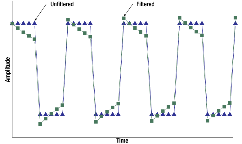
Figure 3: Some modulated signals, including the blue curve plotted above, have no DC component, but they do have non-negligible low-frequency components. When this signal is high-pass filtered by an AC coupling, the resulting signal is distorted. The green curve is one example of this.
Click to Enlarge
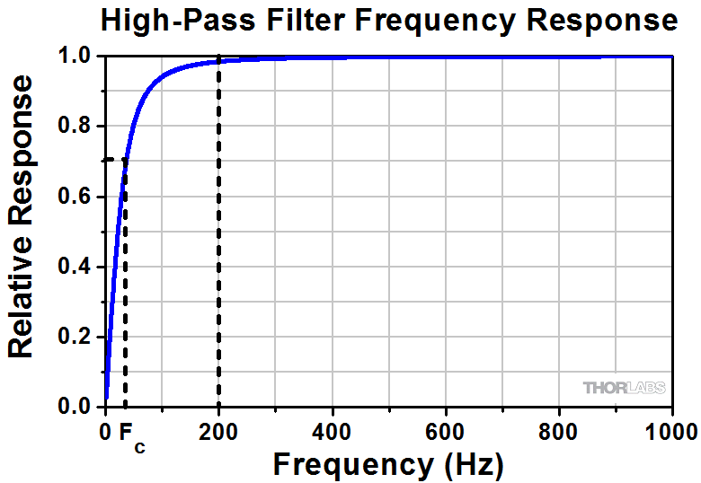
Figure 2: This frequency response magnitude plotted above models a capacitor-based high-pass filter. Its cutoff frequency (Fc) is 35 Hz, and it was used to filter the signal plotted in Figure 3. That signal has a repetition rate of 200 Hz.
Reasons to Use the AC Coupled Input
By rejecting the signal's DC component, AC coupling can reduce the total amplitude of the signal. This can increase the measurement resolution provided by the instrument, as well as overcome saturation and clipping problems. AC coupling provides good results when information is carried by high frequency signal components and low frequency components are not of interest. AC coupling can also be preferred when the application does not tolerate DC frequency signal components, as is the case for some telecommunications applications.
When Using the AC Coupled Input
If AC coupling is used, it is important to keep in mind that this coupling acts as a high pass filter and affects the frequency content of the signal.
As illustrated by Figure 2, this coupling does not just remove the DC offset, it can also attenuate low frequency components that may be of interest. Due to this, AC coupling can result in signal distortion. To illustrate the effects of high-pass filtering, Figure 3 plots a binary signal, with 200 Hz repetition rate, before and after it is filtered by the high-pass filter with 35 Hz cutoff frequency (Fc).
AC-coupled, digital telecommunications signals mitigate this problem by ensuring the signals are DC balanced, so that they have no DC offset. If the signals were not DC balanced, a series of ones could cause a sustained high signal level. This would introduce a non-zero DC level that would cause the signal to be affected by the capacitive filtering. The result could be bit errors due to high states being incorrectly read as low states.
Date of Last Edit: Dec. 4, 2019
| Posted Comments: | |
yazhou wang
(posted 2020-11-20 11:44:14.55) Hi,
The required input impedance for the voltage amplifier is 50 Ω or 1 MΩ? From the document (https://www.thorlabs.com/drawings/8678fb6aca75975b-F37F8116-AAB5-9537-98C0573F4C042CE1/AMP220-SpecSheet.pdf ), you can see the input Impedance is 1 MΩ in the Specifications table. However, in the AC Performance Table part, there is a item 'Bandwidth (3 dB, Rin: 50 Ω, Cin: 100 pF)'. This means the input impedance should be 50 Ω?
Thanks.
Best regards,
Yazhou MKiess
(posted 2020-11-24 06:32:06.0) Thank you very much for your feedback. The input resistance of this voltage amplifiers is 1MOhm. The calculated bandwidth, which is shown in the specification sheet, is for a source with 50Ohm. The performance of the AMP is best for a low impedance source - in this example: 50Ohm. |

 Zoom
Zoom| Key Specsa | ||||||||
|---|---|---|---|---|---|---|---|---|
| Item # | Voltage Gain | Bandwidth | Rise/Fall Time (10% to 90%) |
Input Voltage Limits |
Output Voltage Range |
Output Impedance |
Mass (Weight) |
|
| AMP220 | 10 V/V | DC to 100 kHz | <3 µs | ±200 mV | ±1 V (50 Ω Load) ±2 V (Hi-Z Load) |
50 Ω | 80 g (2.8 oz) |
|
| AMP210 | 1000 V/V | ±2 mV | ||||||
| AMP200 | 10 V/V, 100 V/V, or 1000 V/Vb |
±200 mV @ 10 V/V ±20 mV @ 100 V/V ±2 mV @ 1000 V/V |
||||||

 Zoom
Zoom
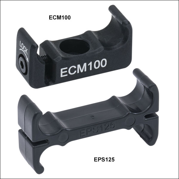
Aluminum Clamps, Post Mountable
These anodized aluminum clamps provide secure mounting for the amplifiers sold above. The clamp can snap onto the side of the device and the flexure lock can be tightened using the 2 mm (5/64") hex locking screw on the side. The ECM100 fits onto the 1.00" side, while the ECM125 fits onto the 1.25" side.
Each clamp has a #8 (M4) counterbore on the bottom, allowing it to be mounted on a Ø1/2" post or any surface with an 8-32 (M4) tap. The clamp must be mounted via the counterbore before the device is attached, as the counterbore will not be accessible once the housing is secured in the clamp.
Plastic Clamp, Double Sided
The EPS125 clamp is designed to connect two rectangular housings for compact setups; the clamp attaches to the 1.25" side of each device.