Intensity Noise Analyzer, USB Powered
- Low Quiescent Noise Floor: <-140 dBV2/Hz
- Onboard Calculation of the Relative Intensity Noise
- Powered and Controlled via USB 2.0
- 9 Hz Minimum Resolution Bandwidth for Resolving Low-Frequency Noise Sources
PNA1
Intensity Noise Analyzer
Application Idea
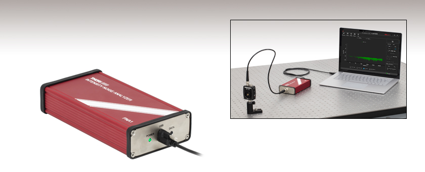
A typical optical setup for frequency-domain measurements. The output of the DET10A2 silicon detector is connected to the PNA1 noise analyzer using a BNC cable (Item # 2249-C-24). The PNA1 is powered via USB 2.0 and operated with the Intensity Noise Analyzer Software.

Please Wait
| Key Specificationsa | ||
|---|---|---|
| Quiescent Noise Floorb | <-140 dBV2/Hz | |
| Broadband Noise Densityc | <60 nV/√Hz | |
| Bandwidth | DC to 3 MHz | |
| Nominal Input Sampling Resolution | 18 Bit | |
| Sample Rates | 12.5 MHz, 781.25 kHz, 48.83 kHz | |
| Resolution Bandwidthd | 390 kHz - 3 MHz | 2.3 kHz |
| 24.5 kHz - 390 kHz | 140 Hz | |
| DC - 24.5 kHz | 9 Hz | |
The PNA1 Noise Analyzer is commonly used to analyze signals from the following devices:
- Biased Detectors
- Amplified Detectors
- Photomultiplier Tubes (PMTs)
- Monitor Ports for Electronic Equipment
- Strain Gauges
- Accelerometers
- Microphones
Click to Enlarge
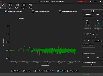
The Intensity Noise Analyzer software provides a simple GUI to control the PNA1 noise analyzer. Measurements can be displayed in either the frequency or time domain.
Features
- High-Precision, Low-Noise Intensity Noise Analyzer for Frequencies Up to 3 MHz
- Multiple Sample Rates for Optimized Resolution Bandwidth (See Table to the Right)
- Input Voltage Range: ±3.85 V
- BNC Signal Input, Internally Terminated with a 10 kΩ Impedance
- Operated with Intensity Noise Analyzer Software (See Software Tab for Software Download)
- Displays Data in Frequency or Time Domain
- Frequency-Domain Readout with Power Spectral Density or Relative Intensity Noise (RIN) Units
- Calculates the Total Integrated Relative Intensity Noise (IRIN)
- Requires a User-Supplied Computer (See Software Tab for Details)
Applications
- Laser Relative Intensity Noise Characterization
- Detection of Noise in Optical Setups (Acoustic Noise, Electrical Noise, Vibration Noise)
- Determining Best Frequencies for Lock-In Detection
- CARS, SRS, or Transient Absorption System Diagnostics
- Error Signal Frequency-Domain Optimization (PID Parameters)
- Spectral Analysis of Laboratory Voltage or Current Signals
Thorlabs' PNA1 Intensity Noise Analyzer (INA) is a high-precision (18-Bit Analog-to-Digital Conversion) instrument used to measure intensity noise in optical systems. Featuring a DC to 3 MHz input frequency bandwidth, this device overlaps data from several sample rates to optimize resolution bandwidth and provide high frequency-axis resolution over its full bandwidth (see table to the right); the 9 Hz minimum resolution bandwidth is ideal for resolving low-frequency noise sources. With a nominal noise floor less than -140 dBV2/Hz, this low-noise instrument is designed to identify environmental noise sources, such as ambient lighting or electrical line noise, in an optical experiment. Ideal applications also include light source and instrumentation development, where characterizing noise levels or detection limits is critical; see the Application tab for an example measurement.
When connected to a voltage source through the co-axial input on the front panel of its housing (see the Front & Back Panels tab), the INA samples the input signal with 18-bit resolution. The device can be used with a voltage input up to ±3.85 V and a maximum of 100 mA of current. Common voltage sources include transducers, such as a photodiode used to measure the output of an optical setup, and monitor outputs of electronic equipment. This input is internally terminated with a 10 kΩ impedance; lower input impedances can be achieved by adding on a feed-through terminator, such as the T4119 50 Ω BNC feed-through terminator. For applications requiring a battery-biased photodiode, we recommend using the VT2 variable resistance BNC feed-through terminator.
To provide high frequency-axis resolution at low frequencies, data acquisition occurs at three separate sample rates: 12.5 MHz, 781.25 kHz, and 48.83 kHz. Both the signal conditioning hardware and digital logic design of the INA are optimized for low noise, high-resolution data acquisition. This data is transmitted to a user-supplied PC over a hi-speed USB 2.0 connection.
The PNA1 noise analyzer is powered using the mini-B USB port on the back panel of the housing, which is connected to a Hi-Speed PC USB type-A port. This also provides the USB 2.0 protocol needed to control the device. A USB-ABL-60 USB 2.0 type-A to mini-B cable with a locking screw is included with each device.
Power and Data LED indicators are included on the front panel to easily identify the operation status of the PNA1 noise analyzer. When the device is powered on but not in use, the Power LED is lit and the Data LED is off; the Data LED will be solidly illuminated green when the device is transmitting data.
Software
The PNA1 noise analyzer is operated using the Thorlabs' Intensity Noise Analyzer software. The user-friendly interface included controls for starting and stopping a measurement, and it can display this data in either the frequency or the time domain. Users may choose between visualizing frequency domain data as either Power Spectral Density (PSD) or Relative Intensity Noise (RIN). For more information on the required software, please see the Software tab.
Grounding
Please note that care must be taken to avoid grounding loops, which can cause irregular behavior at the measurement output for low frequencies; details for several ground loop scenarios can be found in the manual. Avoid contacting the nickel-plated end plates of the housing, which are conductive to the device's internal signal ground, with an earth-grounded table.
Click to Enlarge
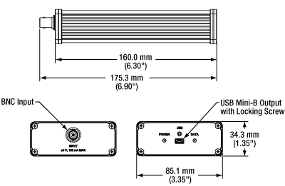
PNA1 Intensity Noise Analyzer Dimensions
| Item # | PNA1 | |
|---|---|---|
| Operating Specifications | ||
| Quiescent Noise Floora | <-140 dBV2/Hz | |
| Broadband Noise Densityb | <60 nV/√Hz | |
| Bandwidth | DC to 3 MHz | |
| Nominal Input Sampling Resolution | 18 Bit | |
| Measurable Input Signal Voltagec | ±3.85 V | |
| Maximum Input Voltage | ± 4 V | |
| Maximum Input Current | 100 mA | |
| Sample Rates | 12.5 MHz, 781.25 kHz, 48.83 kHz | |
| Resolution Bandwidthd | 390 kHz - 3 MHz | 2.3 kHz |
| 24.5 kHz - 390 kHz | 140 Hz | |
| DC - 24.5 kHz | 9 Hz | |
| Input Termination | 10 kΩ | |
| Electrical and Data Specifications | ||
| Supply Voltage from USB | 4.75 - 5.25 VDC | |
| Frequency | DC | |
| Supply Current | 500 mA (Max) | |
| Maximum USB Baud Rate | 480 Mb/s | |
| Temperature Rangee | 0 °C to 70 °C | |
Click to Enlarge
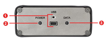
PNA1 Intensity Noise Analyzer Back Panel

Click to Enlarge
PNA1 Intensity Noise Analyzer Front Panel
| Front Panel | |
|---|---|
| Call Out | Description |
| 1 | Signal Input (BNC Female) |
| Back Panel | |
|---|---|
| Call Out | Description |
| 1 | Lockable USB 2.0 Type Mini-B Connector with Threading for Locking Screw |
| 2 | Power Status Indicator LED |
| 3 | USB Status Indicator LED |
Pin Diagrams for the PNA1 Intensity Noise Analyzer
Input Signal
BNC Female
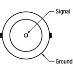
This input accepts a ±3.85 V voltage and 100 mA maximum signal, and it is internally terminated with a 10 kΩ impedance. To achieve lower input impedances, a BNC feed-through terminator can be added on.
Computer Connection
USB Type Mini-B

USB Type Mini-B to Type A Cable Included
| Recommended System Requirements | |
|---|---|
| Operating System | Windows® 10 (Recommended) or 11, 64 Bit Required |
| Memory (RAM) | 4 GB |
| Hard Drive | 300 MB (Min) of Available Disk Space |
| Screen Resolution | 1200 x 800 (Min) |
| Interface | Hi-Speed USB 2.0 |
Software
Version 1.2.0.0 (April 25, 2024)
Click the button below to visit the Intensity Noise Analyzer software page.
Software for the PNA1 Intensity Noise Analyzer
The Intensity Noise Analyzer Software is designed for straightforward control of the PNA1 Intensity Noise Analyzer. The user-friendly GUI includes a readout that can display the data in either the frequency or time domain. Measurement data can be exported as a .csv file.
The GUI has different features for the frequency- and time-domain displays. When using the frequency-domain display, data can be shown as either the Power Spectral Density (PSD) or Relative Intensity Noise (RIN) and users are able to: start and stop a measurement, enable scan averaging, load a reference scan, load a background scan, and display the integrated data. In the time domain, users can start and stop a measurement and select between three scan durations. More information can be found in the manual.
Click to Enlarge
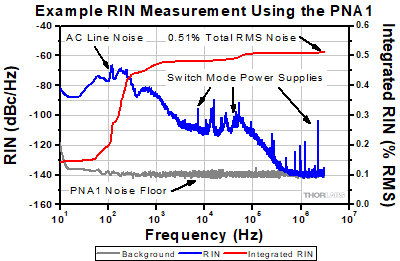
The PNA1 intensity noise analyzer is used to measure the noise from Thorlabs' FSL1030X1 femtosecond fiber laser operating with a 9.3 MHz, 20 W output. The notable peak at approximately 120 Hz in the RIN trace (blue line) indicates noise related to AC power or ground.
Characterizing Noise from a Light Source
For this measurement, an attenuated output beam from Thorlabs' FSL1030X1 1035 nm Ytterbium femtosecond fiber laser (9.3 MHz, 20 W) is incident on a DET10A2 Si photodetector. The photodetector, which outputs a current proportional to the optical power incident on the detector, is connected to the PNA1 intensity noise analyzer via a BNC cable. The noise analyzer then digitizes this voltage at multiple sample rates, digitally filters the time-domain data, performs a discrete Fourier Transform, and normalizes by the DC voltage (calculated as the root mean square voltage). This allows the user to visualize the frequency domain Power Spectral Density (PSD) or Relative Intensity Noise (RIN). For more details on how the PNA1 noise analyzer operates, please see the Operation tab.
The graph to the right shows the results of the measurement described above. The background trace (gray line) indicates the quiescent noise floor of the measurement setup, without the laser or the photodetector energized. The signal levels shown in the background trace effectively define the lower limit of signals that can be recognized using the PNA1 noise analyzer. The blue line shows the RIN of the light source over the bandwidth of the device. A notable peak exists at roughly 120 Hz, which for electrical systems operated in the United States, typically indicates noise related to AC power or ground. The integrated RIN (red line) with the DC offset subtracted is 0.51% and would typically be considered a favorable noise level for a system of this power and pulse width.
Click to Enlarge
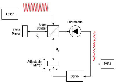
This schematic shows a phase-locked loop consisting of a Michelson interferometer with a photodiode for producing an error signal, a PNA1 analyzer, and a servo feeding back to an adjustable mirror in one of the arms.
Optimizing a Phase-Locked Loop
Many techniques in photonics require locking two different oscillating sources to be in phase with each other. This is typically achieved by creating a signal that is sensitive to the phase difference between the two sources and feeding back on one of the sources to “lock” the two together. Usually, one of the oscillators is the reference and is assumed to be very low noise, and the other oscillator is locked to this reference. Such a phase-locked loop (PLL) cannot perfectly correct for the phase deviations between the two sources, so when optimizing the lock, it is crucial to be able to measure and analyze the phase error (phase noise) between the two sources. A PNA1 analyzer added to a PLL provides a convenient way to visualize and quantify the quality of a lock and aids in optimization.
As an example, a PLL can be constructed to lock two optical path lengths together, as shown in the schematic to the right. A beam splitter is used to create a Michelson interferometer with one fixed mirror and one adjustable mirror. The reflected beams are combined by the splitter, and a photodiode functions as a low-pass filter to generate an error signal proportional to the path length difference. The error signal is passed into a servo that feeds back to the adjustable mirror to lock the length of the two interferometer arms together. Using a PNA1 analyzer for optimization, it is possible to lock the path lengths in such a setup to within approximately the radius of a hydrogen atom. For more information on phase-locked loops and experimental results from a path length lock, see this app note.
Operation
It is often useful to isolate sources of noise in an experiment by identifying signal components in the frequency domain, where each measured amplitude is represented as a function of frequency. The PNA1 Intensity Noise Analyzer performs this process of transforming the signal into a frequency-domain representation. The basic theory of operation for the noise analyzer is detailed below.
Click to Enlarge
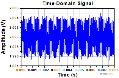
Figure 1: Simulation of a time-domain measurement with noise.
Click to Enlarge
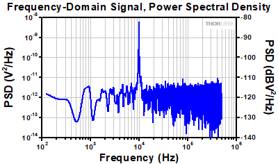
Figure 2: Power Spectral Density trace for the curve shown in Figure 1. Note the significant peak at the 10 kHz signal frequency.
Click to Enlarge
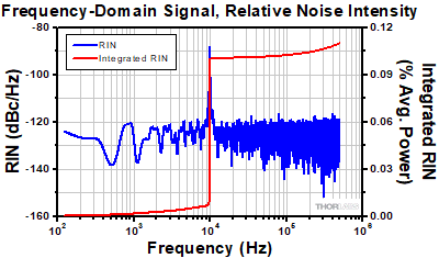
Figure 3: RIN trace (blue) obtained by normalizing the PSD trace in Figure 2 by the RMS power in the signal with the frequency-wise integrated RIN trace superimposed (red). Note the significant inflection point in the integrated RIN curve at the signal frequency, which represents a 0.10% increment in integrated noise. The noise from the Gaussian white noise adds in quadrature with the 10 kHz signal to a final percentage of roughly 0.11% integrated RIN.
Time-Domain Measurement
The PNA1 samples the input signal from a voltage source, such as photodiode. This time-domain measurement, which shows the voltage sampling as function of time, is equivalent to what would be observed if the output signal from the voltage source was displayed on an oscilloscope.
Figure 1 shows a simulated time-domain measurement. This sine wave has the following properties: 2.000 V DC offset, 2.8284 mV wave amplitude (2 mV RMS), and 10 kHz frequency. The random noise on the signal is Gaussian with a 0.0009 V RMS voltage.
Frequency-Domain Representation
To determine the frequency components of the signal, the PNA1 noise analyzer converts time-domain data to the frequency domain using a Fast Fourier Transform (FFT). The result of an FFT, which is a fast means of calculating a Discrete Fourier Transform (DFT), is a complex number whose real component represents the cosine amplitude of the digitized voltage signal and whose imaginary component represents the sine amplitude of the digitized voltage signal. The FFT for an equally spaced series of N time-domain data points, x[n], is given as:

where X[k] is a vector of complex numbers representing the sine and cosine components of the time-domain signal at an index k, j is an imaginary number, and n denotes a zero-referenced index in the time-series data. Please note that each k index represents one equal division of the sample rate of the acquired signal.
The magnitude of the input signal at the frequency relevant to index k, Y[k], is given as:

This is used to determine the total signal power at one frequency index k, which is given as 2(Y[k])2. However, it is generally preferred to work with the power spectral density (PSD), which is the density of power at a given frequency index. PSD is calculated by the PNA1 noise analyzer according to:

where fs is the sample frequency and N is the number of samples in the time-domain signal. PSD, in the context of the PNA1 noise analyzer, has units of V2/Hz. Figure 2 shows the PSD trace for the curve in Figure 1. As expected for a sine wave with a 10 kHz signal frequency, the frequency-domain representation shows a significant peak at 10 kHz.
Relative Intensity Noise
While the PSD provides the density of power at a given frequency index, the noise in a system can be more intuitively understood using the relative intensity noise (RIN). RIN is the PSD normalized by the total power in the time-domain signal. In the case of the PNA1 intensity noise analyzer, RIN[k] is defined as:

where PSD[k] is the power spectral density at a frequency index k and VRMS is the Root Mean Square (RMS) voltage of the time-domain signal. VRMS can be computed as:

where V[n] is the voltage at a specific time-domain index. RIN typically has units of dBc/Hz, which is the power in dB below the carrier per unit bandwidth. For a measurement where the majority of the signal is a DC value, i.e. measurement of the output power of a CW laser, the carrier is equivalent to the DC power and VRMS can be approximated as the DC offset voltage.
The integrated RIN, RINint, in a frequency-domain data series may be obtained by integrating these values over the frequency span of the spectral data:

where fn is the Nyquist frequency of the time-domain data, which is one half the sample rate. This RIN value is in electrical power units (V2). To convert the RINint into a percentage noise (for example, when a laser is detected by a photodiode), the software takes the square root to convert back to linear voltage units (V) and multiplies by 100, which yields the percentage intensity noise on the optical signal into the photodiode.
Frequency Tiering
The spacing of points on the frequency axis of a DFT is often referred to as the resolution bandwidth (RBW). This figure is simply the ratio of the sample rate of the time data, Fs , prior to performing the DFT, to the number of points in the time-series data, N:

where Kw is a correction factor to account for the effect of any windowing operation. This correction factor is a secondary consideration in resolution bandwidth. The windowing operation has the effect of spreading out the signal power in a given frequency segment of the FFT to the adjacent frequency segments, since the approximately sinc-function frequency-domain response of the window function is convolved with the input signal.
Smaller RBW is naturally advantageous when trying to discriminate noise sources close to one another or at low frequencies. To reduce the nominal RBW in the expression shown above, either the number of points in the DFT may be increased or the sample rate may be reduced. To provide useful RBW across the full bandwidth of the PNA1 noise analyzer, three sample rates are used. The initial sample rate of the device is reduced and then reduced again. By so doing, the RBW is adjusted to three separate bandwidths to provide good frequency resolution over the entire five decades of frequency range.
| Posted Comments: | |
Santosh Balakrishnan
(posted 2024-09-20 17:26:03.78) I was trying to follow the steps specified on the operation tab and the user manual to reproduce the PSD and RIN plots from the simulated noisy sinusoidal signal (2V offset, 2mV rms etc.).
As noted by the previous comment, the first equation for PSD is incorrect.
Additionally, my results (with the corrected formula) seem to be about 6 dB different from the plots you have shown- i.e. the calculated PSD has a peak value of ~ -75 dB, while your plot shows a peak value of -81 dB. I've checked with Hanning window as the user manual describes, but that doesn't seem to be cause of this difference.
Additionally, are the integrated RIN percentage values plotted for the integration interval 100 to 500 kHz? tdevkota
(posted 2024-09-27 02:13:03.0) Thank you for contacting Thorlabs. The example plot included in the user manual is generated using a rectangular window and is intended primarily for conceptual demonstration. Any discrepancies observed between the example data and user data may be attributed to differences in the sample rate. The RIN integration interval includes frequencies from 100 to 500 kHz. I've reached out to you directly to discuss this in further details. Dimitrios Tsevas
(posted 2024-07-31 11:13:23.163) The intensity noise analyzer's power LED stays dark when we plug the device's USB cable into some of our laptops. Could it be that it draws too much power and some laptops cannot give it? We would recommend a separate, external power source.
Less importantly, an ethernet connection and a very basic API that can be accessed from python would be nice to measure and read out averaged spectra from any computer on the network. Mikko Narhi
(posted 2024-06-12 09:40:07.043) I'm wondering whether on the "Operation" tab there is an error in the equation for calculating the PSD? It says that to get the PSD from the FFT you need to multiply the mag squared Y[k]^2 by 2N and divide by the sampling rate fs. I believe this should be multiplied by 2 and divided by N x fs ? See e.g. Matlab webpage on Power Spectral Density estimation from FFT jpolaris
(posted 2024-06-14 07:03:39.0) Thank you for contacting Thorlabs. I have confirmed that you are indeed correct. The factor of N that appears in the numerator of the PSD equation that we provide in our "Operation" tab, as well as in the PNA1 manual, should actually appear in the denominator. Thank you for pointing this out to us so that we can make the appropriate corrections to our documentation. Ian Bloomfield
(posted 2023-12-14 06:25:12.48) Hi-
This is a really nice device that strikes a good balance between noisefloor, bandwidth, and dynamic range.
However- for us to utilize this device to the fullest, we would love to see an API so we can automate measurements. Is this on the roadmap?
Thanks! cdolbashian
(posted 2023-12-15 05:26:06.0) Thank you for reaching out to us with this inquiry! We are certainly planning on releasing such a feature for this exact type of application. Bowen Liu
(posted 2023-10-30 20:13:35.203) Hi, I am Bowen from Univ of Tokyo. We have a problem regarding to the PNA1 noise floor that is shown on your product website below "application" tag. When using PNA1 to test the laser RIN performance, we found that the RIN of background noise is always higher than that of signal laser. Even the PD was disconnected with PNA1, the RIN of noise floor (-90 dBc/Hz) is much higher than what you show on your website (-140 dBc/Hz). However, the PSD of noise floor seems fine. We was wondering how you get the RIN of noise floor that shown on your website, and do you normalize it to RMS of voltage? jdelia
(posted 2023-10-31 10:26:54.0) Thank you for contacting Thorlabs. The background noise displays with very high RIN values because there is only a very small DC voltage on the signal when the PD is blocked or disconnected. The RIN calculation normalizes the measured PSD of the electrical signal by the DC voltage, so is dividing by a very small number in the case of no input. If you would like to plot the RIN “background” against measured data you can save the file with the background (i.e. detector blocked or off) and scale the PSD units (V^2/Hz) of the background saved data into the equivalent RIN units of the real measurement by dividing by Vrms^2 saved in the real measurement. This will put both the background and the signal on the same RIN axis. Tobias Hofer
(posted 2023-07-17 13:36:11.95) Hey the application Idea on this picture is strongly misleading, you should terminate with a 50 Ohm resistor or you would limit the BW of most your PDs to below 3MHz. Also: 100mA max current at 10kOhms input? That would be 1kV according to U=R*I? I don't get your instructions on this product. Cheers, Tobias Hofer jdelia
(posted 2023-07-21 02:39:36.0) Thank you for contacting Thorlabs. The optimal termination for any measurement is a function of many parameters, including, as you indicated, the capacitance of the photodiode. The Application Idea picture uses a DET10A2 detector with a typical capacitance of 6 pF. This, along with the 10 kOhm termination, would give a – 3dB bandwidth of approximately 2.65 MHz, which is well-matched to the device maximum operating bandwidth of 3 MHz, although a user may want to choose a different termination if they want less roll-off at the high frequency side of the measurement. Thorlabs fortunately provides many different options for varying the termination, including fixed stub terminators (FTK01), fixed feed-through terminators (T4119), and a variable feed-through terminator (VT2). 50 Ohms would be a good choice for many measurements, although a user may get a higher signal to noise ratio by terminating at a higher resistance (500 Ohm, for example), yielding a higher DC voltage and SNR. For the input current markings, those are absolute maximum ratings. The PNA1 has internal protection circuitry that will sink the excess current (so that the voltage does not rise above the damage point of the internal components), and the maximum rating for that protection circuitry is +/- 100 mA. Brian Anderson
(posted 2023-06-13 18:23:43.227) Hello,
I'm curious if in future version of the software you could additional options to change the calculations.
For example, it would be great if you could include a feature to either subtract the dark current/voltage from the DC value or subtract off a previously measured background noise before automatically calculating the RIN value.
Secondly it would be great if the % RIN could be calculated within a specific frequency range. E.G. calculating the RIN in a small subset (say from 2 Khz to 10 Khz) instead of covering the entire 3 MHz bandwidth.
Thanks,
Brian cdolbashian
(posted 2023-06-20 03:10:59.0) Thank you for reaching out to us with this inquiry! I have passed your feedback along to our responsible software team. |
 Products Home


 Intensity Noise Analyzer