Mounted Photodiodes
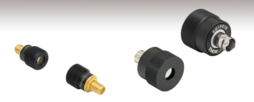
- InGaAs, Si, Black Si, or Ge Photodiodes
- Ideal for Measuring Pulsed and CW Sources
- Housing with External SM05 or SM1 Threading
SM05PD2A
FDS010 Photodiode Mounted in SM05 Externally Threaded Housing
SM1PD1B
FDS1010 Photodiode Mounted in SM1 Externally Threaded Housing

Please Wait
| Mounted and Unmounted Detectors |
|---|
| Photodiodes |
| Mounted Photodiodes (200 - 1800 nm) |
| Unmounted Photodiodes (200 - 2600 nm) |
| Pigtailed Photodiodes (320 - 1000 nm) |
| Calibrated Photodiodes (350 - 1800 nm) |
| Photovoltaic Detectors (2000 - 10 600 nm) |
| Thermopile Detectors (190 - 20 000 nm) |
| Pyroelectric Detector (600 - 16 000 nm) |

Click to Enlarge
Figure 1.2 The PBM42 Bias Module Used to Apply an External Reverse Bias Voltage to the SM1PD2A Photodiode
Thorlabs offers silicon (Si), black silicon (b-Si), indium gallium arsenide (InGaAs), or germanium (Ge) photodiodes in convenient externally SM05 (0.535"-40) or SM1 (1.035"-40) threaded tubes. The electrical output of the photodiode is provided through a standard SMA connector (SM05PD Series) or BNC connector (SM1PD Series) for quick connection to the measuring circuit.
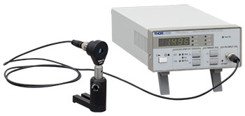
Click to Enlarge
Figure 1.1 PDA200C Benchtop Photodiode Amplifier Connected to
an SM1-Threaded Mounted Photodiode Using a BNC Cable
The mounted photodiodes presented here are compatible with the PDA200C Benchtop Photodiode Amplifier and Thorlabs' Modular Photodiode Amplifiers. The photodiodes come in either a Type A (cathode grounded) or Type B (anode grounded) arrangement. The pin codes for specific items may be found below. All models are ideal for measuring pulsed and CW sources. The insulated external thread on the main body makes these photodiodes compatible with all Thorlabs SM05 and SM1 Mounting Adapters.
Please refer to the tables below for more details on each model and note that these photodiodes are not calibrated. We also offer unmounted calibrated photodiodes.
Please note that inhomogeneities at the edges of the active area of the detector can generate unwanted capacitance and resistance effects that distort the time-domain response of the photodiode output. Thorlabs therefore recommends that the incident light on the photodiode is well centered on the active area. This can be accomplished by placing a focusing lens or pinhole in front of the detector element.
For applying an external bias voltage to these photodiodes, we offer the PBM42 bias module (sold below), which is compatible via adapters with all of the photodiodes on this page and is shown in Figure 1.2.
For information on the photodiode saturation limit and the noise floor, as well as a collection of Thorlabs-conducted experiments regarding spatial uniformity (or varying responsivity) and dark current as a function of temperature, refer to the Lab Facts tab. The Photodiode Tutorial provides more general information regarding the operation, terminology, and theory of photodiodes.
Thorlabs offers spectral-flattening filters that are designed to improve the response uniformity of our silicon photodiodes. Click here to learn more.
Photodiode Tutorial
Theory of Operation
A junction photodiode is an intrinsic device that behaves similarly to an ordinary signal diode, but it generates a photocurrent when light is absorbed in the depleted region of the junction semiconductor. A photodiode is a fast, highly linear device that exhibits high quantum efficiency and may be used in a variety of different applications.
It is necessary to be able to correctly determine the level of the output current to expect and the responsivity based upon the incident light. Depicted in Figure 100A is a junction photodiode model with basic discrete components to help visualize the main characteristics and gain a better understanding of the operation of Thorlabs' photodiodes.

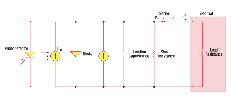
Figure 100A Photodiode Model
Photodiode Terminology
Responsivity
The responsivity of a photodiode can be defined as a ratio of generated photocurrent (IPD) to the incident light power (P) at a given wavelength:

Modes of Operation (Photoconductive vs. Photovoltaic)
A photodiode can be operated in one of two modes: photoconductive (reverse bias) or photovoltaic (zero-bias). Mode selection depends upon the application's speed requirements and the amount of tolerable dark current (leakage current).
Photoconductive
In photoconductive mode, an external reverse bias is applied, which is the basis for our DET series detectors. The current measured through the circuit indicates illumination of the device; the measured output current is linearly proportional to the input optical power. Applying a reverse bias increases the width of the depletion junction producing an increased responsivity with a decrease in junction capacitance and produces a very linear response. Operating under these conditions does tend to produce a larger dark current, but this can be limited based upon the photodiode material. (Note: Our DET detectors are reverse biased and cannot be operated under a forward bias.)
Photovoltaic
In photovoltaic mode the photodiode is zero biased. The flow of current out of the device is restricted and a voltage builds up. This mode of operation exploits the photovoltaic effect, which is the basis for solar cells. The amount of dark current is kept at a minimum when operating in photovoltaic mode.
Dark Current
Dark current is leakage current that flows when a bias voltage is applied to a photodiode. When operating in a photoconductive mode, there tends to be a higher dark current that varies directly with temperature. Dark current approximately doubles for every 10 °C increase in temperature, and shunt resistance tends to double for every 6 °C rise. Of course, applying a higher bias will decrease the junction capacitance but will increase the amount of dark current present.
The dark current present is also affected by the photodiode material and the size of the active area. Silicon devices generally produce low dark current compared to germanium devices which have high dark currents. Table 100B lists several photodiode materials and their relative dark currents, speeds, spectral ranges, and costs.
| Table 100B Photodiode Materials | ||||
|---|---|---|---|---|
| Material | Dark Current | Speed | Spectral Range | Cost |
| Silicon (Si) | Low | High Speed | Visible to NIR | Low |
| Black Silicon (B-Si) | Low | Medium Speeda | Visible to NIR | Moderate |
| Germanium (Ge) | High | Low Speed | NIR | Low |
| Indium Gallium Arsenide (InGaAs) | Low | High Speed | NIR | Moderate |
| Indium Arsenide Antimonide (InAsSb) | High | Low Speed | NIR to MIR | High |
| Extended Range Indium Gallium Arsenide (InGaAs) | High | High Speed | NIR | High |
| Mercury Cadmium Telluride (MCT, HgCdTe) | High | Low Speed | NIR to MIR | High |
Junction Capacitance
Junction capacitance (Cj) is an important property of a photodiode as this can have a profound impact on the photodiode's bandwidth and response. It should be noted that larger diode areas encompass a greater junction volume with increased charge capacity. In a reverse bias application, the depletion width of the junction is increased, thus effectively reducing the junction capacitance and increasing the response speed.
Bandwidth and Response
A load resistor will react with the photodetector junction capacitance to limit the bandwidth. For best frequency response, a 50 Ω terminator should be used in conjunction with a 50 Ω coaxial cable. The bandwidth (fBW) and the rise time response (tr) can be approximated using the junction capacitance (Cj) and the load resistance (RLOAD):

Noise Equivalent Power
The noise equivalent power (NEP) is the input signal power that results in a signal-to-noise ratio (SNR) of 1 in a 1 Hz output bandwidth. This is useful, as the NEP determines the ability of the detector to detect low level light. In general, the NEP increases with the active area of the detector and is given by the following equation:

Here, S/N is the Signal to Noise Ratio, Δf is the Noise Bandwidth, and Incident Energy has units of W/cm2. For more information on NEP, please see Thorlabs' Noise Equivalent Power White Paper.
Terminating Resistance
A load resistance is used to convert the generated photocurrent into a voltage (VOUT) for viewing on an oscilloscope:

Depending on the type of the photodiode, load resistance can affect the response speed. For maximum bandwidth, we recommend using a 50 Ω coaxial cable with a 50 Ω terminating resistor at the opposite end of the cable. This will minimize ringing by matching the cable with its characteristic impedance. If bandwidth is not important, you may increase the amount of voltage for a given light level by increasing RLOAD. In an unmatched termination, the length of the coaxial cable can have a profound impact on the response, so it is recommended to keep the cable as short as possible.
Shunt Resistance
Shunt resistance represents the resistance of the zero-biased photodiode junction. An ideal photodiode will have an infinite shunt resistance, but actual values may range from the order of ten Ω to thousands of MΩ and is dependent on the photodiode material. For example, and InGaAs detector has a shunt resistance on the order of 10 MΩ while a Ge detector is in the kΩ range. This can significantly impact the noise current on the photodiode. For most applications, however, the high resistance produces little effect and can be ignored.
Series Resistance
Series resistance is the resistance of the semiconductor material, and this low resistance can generally be ignored. The series resistance arises from the contacts and the wire bonds of the photodiode and is used to mainly determine the linearity of the photodiode under zero bias conditions.
Common Operating Circuits
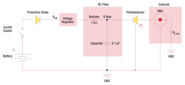
Figure 100C Reverse-Biased Circuit (DET Series Detectors)
The DET series detectors are modeled with the circuit depicted in Figure 100C. The detector is reverse biased to produce a linear response to the applied input light. The amount of photocurrent generated is based upon the incident light and wavelength and can be viewed on an oscilloscope by attaching a load resistance on the output. The function of the RC filter is to filter any high-frequency noise from the input supply that may contribute to a noisy output.
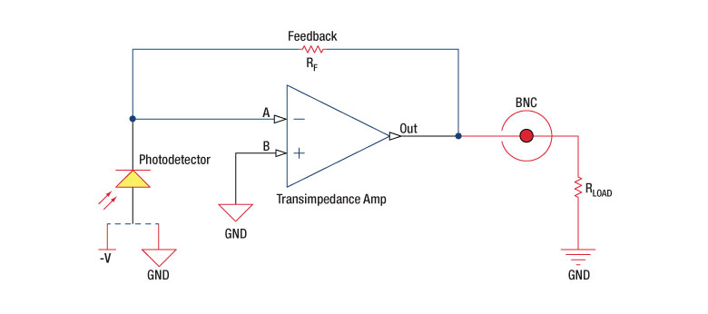
Figure 100D Amplified Detector Circuit
One can also use a photodetector with an amplifier for the purpose of achieving high gain. The user can choose whether to operate in Photovoltaic of Photoconductive modes. There are a few benefits of choosing this active circuit:
- Photovoltaic mode: The circuit is held at zero volts across the photodiode, since point A is held at the same potential as point B by the operational amplifier. This eliminates the possibility of dark current.
- Photoconductive mode: The photodiode is reversed biased, thus improving the bandwidth while lowering the junction capacitance. The gain of the detector is dependent on the feedback element (Rf). The bandwidth of the detector can be calculated using the following:
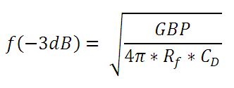
where GBP is the amplifier gain bandwidth product and CD is the sum of the junction capacitance and amplifier capacitance.
Effects of Chopping Frequency
The photoconductor signal will remain constant up to the time constant response limit. Many detectors, including PbS, PbSe, HgCdTe (MCT), and InAsSb, have a typical 1/f noise spectrum (i.e., the noise decreases as chopping frequency increases), which has a profound impact on the time constant at lower frequencies.
The detector will exhibit lower responsivity at lower chopping frequencies. Frequency response and detectivity are maximized for
![]()
Figures 3.1 and 3.2 show examples of electrical circuits that can be used in conjunction with our mounted diodes. Our mounted photodiodes with SM05-threaded (0.535"-40) housings utilize an SMA connector type whereas those with SM1-threaded (1.035"-40) housings have a BNC connector type. Figure 3.1 depicts a cathode-grounded photodiode with an example circuit. This is a reverse bias configuration with a positive voltage output. Figure 3.2 depicts an anode-grounded photodiode with an example circuit. Note that in this instance, the polarity of the power source has been reversed. Figure 3.2 is also a reverse bias configuration but will have a negative voltage output.
The major difference between the configurations shown in Figures 3.1 and 3.2 is the range of the output voltage. Figure 3.1 will output 0 to +V volts, whereas Figure 3.2 will output -V to 0 volts. For more information on photodiode circuits, values, and theory please see the Photodiode Tutorial tab

Figure 3.1 SM05- and SM1-Threaded Mounted Photodiodes, Cathode Grounded

Figure 3.2 SM05- and SM1-Threaded Mounted Photodiodes, Anode Grounded
Summary
This tab contains a collection of experiments performed at Thorlabs regarding the performance of photodiodes we offer. Each section is its own independent experiment, which can be viewed by clicking in the appropriate box below. Photodiode Saturation Limit and Noise Floor explores how different conditions, including temperature, resistivity, reverse-bias voltage, responsivity, and system bandwidth, can affect noise in a photodiode's output. Photodiode Spatial Uniformity explores variations in the responsivity as a small-diameter light beam is scanned across the active area of the photodiode. Photodiodes with different material compositions are tested, and eight units of one silicon-based model are tested to investigate unit-to-unit variations. Dark Current as a Function of Temperature and Noise Equivalent Power (NEP) as a Function of Temperature describe how dark current and NEP, respectively, vary with temperature and how measurements are affected. Beam Size and Photodiode Saturation shows how the photodiode saturation point changes with the incident beam size and investigates several models to explain the results. Bias Voltage examines the effects of incident power on the effective reverse bias voltage of a photodiode circuit and verifies a reliable model for predicting those changes.
Photodiode Saturation Limit and Noise Floor
Click to Enlarge
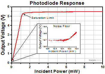
Figure 171A Overview of the Photodiode's Response Curve,
Highlighting the Saturation Limit and the Noise Floor
We present laboratory measurements of the saturation limit and noise floor of a Thorlabs silicon photodiode. While all photodiodes function similarly, there are a number of parameters that affect the noise floor and saturation limit of a photodiode including the sensor temperature, resistivity, reverse bias voltage, responsivity, and system bandwidth. Here we investigated the effect of reverse bias voltage and load resistance within a silicon-based photodiode detection system. Increasing the reverse bias increased the saturation limit and had minimal effect on the noise floor. Decreasing the load resistance decreased the noise floor until reaching the noise of the measurement system, but also decreased the saturation limit. These results demonstrate some of the considerations necessary for choosing the reverse bias voltage and load resistance, and emphasize that noise sources within all of the components must be considered when creating a detection system.
For our experiment we used the FDS100 Si Photodiode as the photodiode under investigation. The collimated output of a fiber-pigtailed laser diode was used as the light source with output power from 0 to 50 mW. The collimated beam was incident upon a beamsplitter that transmitted the majority of the light to the photodiode under investigation and reflected the rest towards a reference power sensor. The photodiode response was then evaluated under various resistive loads and with different reverse bias voltages.
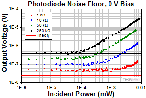
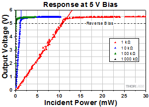
Figures 171A through 171D summarize the measured results for the various tested configurations. From these graphs the changes to the photodiode's linear response, noise floor, and saturation limit can be observed under different reverse voltage biases and load resistances. Figure 171A provides an overview of the photodiode response with a reverse voltage bias of 5 V and resistive load of 10 kΩ. The photodiode saturated at the upper limit of the response when the output photovoltage approached the reverse bias voltage. The noise floor at the lower limit of the response was a result of dark current and the thermal noise from the resistive load (Johnson noise). Figure 171B summarizes the results obtained using the photodiode with a 1 kΩ resistive load and various reverse bias voltages. It illustrates that the saturation limit can be raised by increasing the reverse bias voltage (within specification). Figure 171C summarizes the results from using the photodiode with a 5 V reverse bias voltage and various resistive loads. It illustrates that the slope of the photovoltage response increased as the load resistance was increased. Figure 171D summarizes the noise floor results obtained using a 0 V reverse bias voltage and various resistive loads. The noise floor increased when larger load resistances were used. It is important to note that the 1 kΩ data was measured above the theoretical Johnson noise due to the voltage noise within the measurement system. Minimal change in the overall noise floor was seen when using a 5 V reverse bias voltage. For details on the experimental setup employed and these summarized results, please click here.
Click to Enlarge
Figure 171D Noise Floor with Various Resistive Loads
Click to Enlarge
Figure 171C Response with Various Resistive Loads
Photodiode Spatial Uniformity
 Click to Enlarge
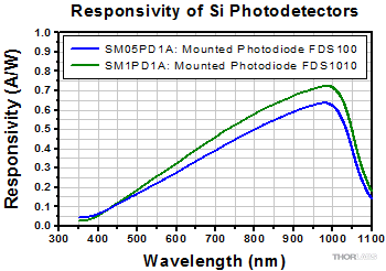
Figure 171E Responsivity, which describes the relationship between the strength of the photocurrent output by the photodetector and the optical power in the incident beam, is dependent on the wavelength of the incident light.
Do all regions of a photodiode's active area have the same responsivity?
The output signal strength from a photodetector is significantly affected by the optical power and wavelength of the incident light. A measure of this relationship is responsivity, which is the magnitude of the output photocurrent divided by the optical power of the incident light. While responsivity has units of ampere per watt, it also varies with wavelength. Often overlooked is that responsivity can also vary as different regions of the photodiode's active area are illuminated.
This work investigated the change in photodetector response as a light beam, with a diameter that was small in comparison to the active area of the photodiode, was scanned across the active area. A selection photodetectors, based on mounted gallium phosphide (GaP), silicon (Si), indium gallium arsenide (InGaAs), or germanium (Ge) photodiodes, were tested.
Responsivity is Wavelength Dependent1,2
One reason responsivity varies with respect to wavelength is the relationship among optical power, wavelength, and photo-generated electrons. A light beam illuminating a surface provides an optical power equal to the energy in the beam divided by the time the surface was illuminated. The energy in a single-wavelength beam equals the number of incident photons times the energy of a single photon. Decreasing the wavelength of the light increases the energy of the photons. If the wavelength is decreased, but the optical power is kept the same, there are fewer incident photons.
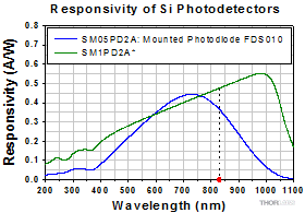
A single photon can generate no more than a single electron of photocurrent in these photodetectors. Due to this, reducing the wavelength of the incident light while holding its optical power constant results in a reduced photocurrent. Since responsivity relates the output photocurrent to the incident optical power, instead of to the number of incident photons per unit time, responsivity is lower at lower wavelengths. The responsivity curves plotted in Figure 171E are examples showing responsivity increasing with wavelength.
The upper wavelength of a photodetector's responsivity is limited by inherent properties of the semiconductor material. In order for an incident photon to contribute to the photocurrent, the photon must have enough energy to free an electron from its bonds to its host atom. Photons with wavelengths above the upper wavelength limit do not have enough energy. The semiconductor material composing the photodiode determines the wavelength of this limit.
Response May Vary as Different Regions of the Photodiode's Active Area are Illuminated1,2
An electron that has escaped the bonds of its host atom by absorbing the energy of a photon is a photo-generated electron. A photo-generated electron contributes to the photocurrent only if the electron is able to successfully travel from where it was generated, across the semiconductor material, and to an electrical contact. A photo-generated electron does not contribute to the photocurrent if it is re-absorbed by the semiconductor material before reaching a contact, which is a more likely outcome if the electron encounters a defect.
Defects are places where the semiconductor's crystal lattice is not perfect. These locations include dislocations, impurities, and voids in the crystal lattice. The external surfaces of a real crystal with finite dimensions are also imperfections, since a perfect crystal is infinite in length, height, and width. Defects in the semiconductor crystal absorb photo-generated electrons at a high rate and turn their kinetic energy into heat, rather than allow the electrons to contribute to the photocurrent.
Electrons generated near defects are more likely to be re-absorbed and less likely to contribute to the photocurrent. While the density of defects in a semiconductor can be minimized, the semiconductor crystals used in photodiodes are not perfect. It is also not unusual for the density of defects to vary throughout the volume of the semiconductor crystal, as well as for the growth of some semiconductor materials to be more prone to forming defects than others.
If the density of defects varies throughout the volume of the semiconductor material, the magnitude of the photocurrent generated within each region would be expected to be different. Since the photodetector's responsivity depends on the magnitude of photocurrent, a varying density of defects would result in the responsivity changing as different locations on the photodetector are illuminated. This effect was investigated using the procedure described in the following section.
Click to Enlarge
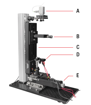
Figure 171F The setup used to measure the change in response across the active area of each photodiode included: a reflective collimator (A), an achromatic doublet lens (B) , vertically-mounted linear translation stage (C), the photodetector under test (D), and two horizontally-mounted translation stages (E) of which one is visible.
Experimental Setup and Results
Measurement Objectives
Several photodetectors were tested to investigate the uniformity of the responsivity across their active areas. The spatially dependent responsivities of one GaP-based, four Si-based, two InGaAs-based, and two Ge-based photodetectors were measured at selected wavelengths. Testing was conducted to investigate the spatial uniformity of the responsivity of:
- All nine photodetector models at a wavelength close to the wavelength of peak responsivity. (Results contained in Table 171G.)
- A Si-based, an InGaAs-based, and a Ge-based photodetector at three different wavelengths. (Results contained in Table 171H.)
- Eight different units of a single Si-based photodetector model at a wavelength close to the wavelength of peak responsivity. (Results contained in Table 171J.)
Experimental Setup (Components Labeled in Figure 171F Are Labeled in the Following)
The experimental setup consisted of a light source (not shown) that was fiber-coupled to an RC12APC-P01 collimator (A), which was installed in a KM100T kinematic mount. An AC254-150-A achromatic doublet lens with a 150 mm focal length (B), which was installed in a ST1XY-D mount, focused the light on the active area of the photodetector (D), which was mounted with the help of a KB1P magnetic quick-release carriage set. Other components in the vertical arm included a previous-generation LTS150 motorized linear translation stage (C), an XT66P1 vertical mounting plate, an XT66-500 66 mm construction rail, and four XT66C4 clamping platforms. The components in the horizontal arm included two previous-generation LNR50S motorized linear translation stages (E), an LNR50P3 XY adapter plate, a baseplate, and two BSC201 closed-loop stepper motor controllers (not shown), which scanned the beam across the active area of the photodetector (D). Most light sources were products from our Superluminescent Diode series. The exception was the 405 nm light source, which was an S3FC405 benchtop laser source.
Procedure
The diameter of the beam was scaled according to the active area of the photodetector, so that approximately 3600 measurements were taken in a 60 x 60 grid across the surface of each photodiode. The beam diameter used for each photodiode was between 50 µm and 500 µm, and the size used to make a particular measurement is included in the notes that accompany each plot in Tables 171G, 171H, and 171J. To view this information, click on the plot of interest.
During the scan, the position of the beam remained stationary, and the two LNR50S motorized stages were used to translate the photodetector in the two directions perpendicular to the optic axis. To ensure that the entire active area of the photodetector was tested, the dimensions of the scan area exceeded the dimensions of the active area.
No reverse bias voltage was applied to any of the photodiodes during this investigation.
Results (Click More [+] to Expand Tables 171G, 171H, and 171J; Click Less [-] to Hide Them)
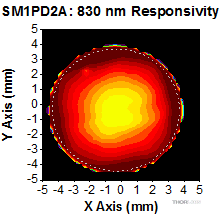
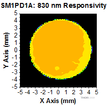
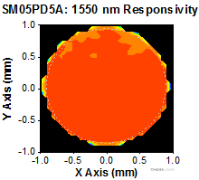
The measurement data were normalized and then plotted with respect to the measurement position. The data in each measurement set were normalized with respect to the value at the center of the active area, which resulted in plots that show the variation of the responsivity across each photodetector's active area and allow the results from these nine different photodetector models to be compared. The plotted data were also processed to remove data points with values indistinguishable from noise. This was done to eliminate data points corresponding to measurements made outside of the active area of each photodetector. However, this approach also removed some measurements made within, but close to, the outer edges of the active areas. The lower photocurrent generated by these regions may have been due to the beam spot partially illuminating regions outside of the active area, as well as photocurrent suppressed by a higher density of defects near the edges.
The plots can be revealed by expanding Tables 171G, 171H, and 171J. Each plot includes a dashed outline surrounding the central 90% of the active area of the photodiode. Under general use, the light beam should remain within this central 90% region to avoid edge effects. Click on each plot to reveal information about the active area of the photodiode and the size of the beam scanned across the active area.
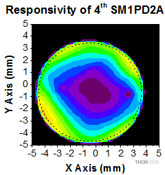
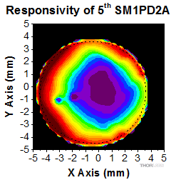
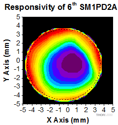
Since these photodetectors represent a small sample size, these measurements are representative of the other photodetectors of its model, but results obtained using other units of the same model may vary. The measurements acquired for these photodetector units were repeatable, but no two semiconductor crystals are identical and unit-to-unit variations should be expected. The following tables show that:
- Table 171G: The variations of the responsivities across the active areas of the Ge-based and GaP-based photodetectors are greater than the variations of the responsivities across the active areas of the Si-based and InGaAs-based photodetectors. This suggests the defect densities of the Si-based and InGaAs-based semiconductor materials are more uniform than the defect densities of the Ge-based and GaP-based semiconductor materials.
- Table 171H: The variations of the responsivities across the active areas of a Si-based, an InGaAs-based, and a Ge-based photodetector change with wavelength. For each photodetector, the minimum spatial variations of the responsivity occurred when the wavelength of light was near the wavelength of the peak value of responsivity.
- Table 171J: Eight units of a single Si-based photodetector model had similar variations of spatial uniformity across their active areas.
| Table 171G All Nine Photodetectors: Uniformity of Response to Light with Near Peak Responsivity Wavelength |
|---|
| Photodetector Measured | Plot of Response Across the Sensor Area to Light of the Indicated Wavelength | Typical Responsivity Plots Measurement Wavelength Indicated |
|
| GaP-Based Photodetector SM05PD7A: Mounted Photodiode FGAP71 |
 Click for Details |
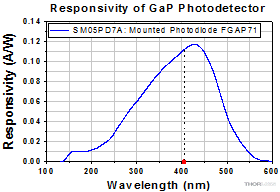 Click to Enlarge |
|
| Si-Based Photodetectors SM05PD2A: Mounted Photodiode FDS010 and SM1PD2A |
 Click for Details |
 Click for Details |
 Click to Enlarge Click to Enlarge |
| Si-Based Photodetectors SM05PD1A: Mounted Photodiode FDS100 and SM1PD1A: Mounted Photodiode FDS1010 |
 Click for Details |
 Click for Details |
 Click to Enlarge Click to Enlarge |
| InGaAs-Based Photodetectors SM05PD5A: Mounted Photodiode FGA21 and SM05PD4A: Mounted Photodiode FGA10 |
 Click for Details |
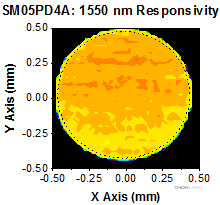 Click for Details |
 Click to Enlarge Click to Enlarge |
| Ge-Based Photodetectors SM05PD6A: Mounted Photodiode FDG1010 and SM1PD5A: Mounted Photodiode FDG03 |
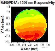 Click for Details |
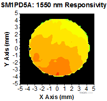 Click for Details |
 Click to Enlarge Click to Enlarge |
| Table 171H Selected Si-, InGaAs-, and Ge-Based Photodetectors: Uniformity of Response of Each to Three Different Wavelengths of Light |
|---|
| Photodetector | Plots of Response Across the Sensor Area to Light of the Indicated Wavelengths | Typical Responsivity Plots Measurement Wavelengths Indicated |
||
| Si-Based Photodetector SM1PD1A: Mounted Photodiode FDS1010 |
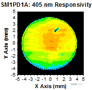 Click for Details Click for Details |
 Click for Details Click for Details |
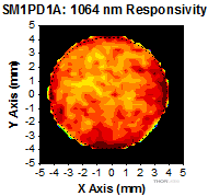 Click for Details Click for Details |
 Click to Enlarge Click to Enlarge |
| InGaAs-Based Photodetector SM05PD5A: Mounted Photodiode FGA21 |
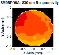 Click for Details Click for Details |
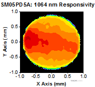 Click for Details Click for Details |
 Click for Details Click for Details |
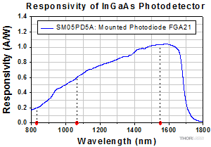 Click to Enlarge Click to Enlarge |
| Ge-Based Photodetector SM1PD5A: Mounted Photodiode FDG1010 |
 Click for Details Click for Details |
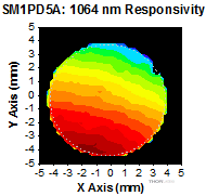 Click for Details Click for Details |
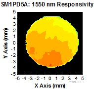 Click for Details Click for Details |
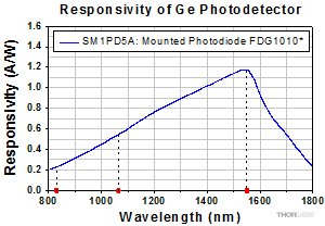 Click to Enlarge Click to Enlarge |
| Table 171J Eight Si-Based SM1PD2A Photodetectors: Uniformity of Response to Light Near Peak Responsivity Wavelength Compared |
|---|
| Eight different Si-based SM1PD2A photodetectors were measured to compare the unit-to-unit variation of the response across the active area. Measurements were performed using 830 nm light, which is close to the wavelength of peak responsivity, as is indicted on the plot. |
 Click to Enlarge |
||
 Click for Details |
 Click for Details |
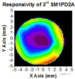 Click for Details |
 Click for Details |
 Click for Details |
 Click for Details |
 Click for Details |
 Click for Details |
References
[1] G. P. Agrawal, Fiber-Optic Communication Systems, 2nd ed., John Wiley & Sons, Inc., New York, 1997. (Particularly Chapter 4)
[2] A. Rogalski, K. Adamiec, and J. Rutkowski, Narrow-Gap Semiconductor Photodiodes, SPIE Press, Bellingham, WA, 2000.
Dark Current as a Function of Temperature
Measurements of dark current as a function of temperature were acquired for several unmounted photodetectors. As is described in the following section, dark current is a relatively small electrical current that flows in p-n junction photodetectors when no light is incident on the detector. Measurements were taken for silicon (Si), germanium (Ge), gallium phosphide (GaP), and indium gallium arsenide (InGaAs) reverse-biased photodiodes over temperatures from 25 °C to approximately 55 °C.
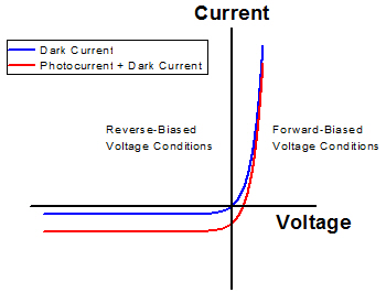
Figure 171K Current-Voltage Characteristic of a P-N Junction
Current-Voltage Characteristics of p-n Junction Photodiodes
The characteristic current-voltage relationship of p-n junction photodiodes, as diagrammed in Figure 171K, possesses forward-biased and reverse-biased voltage regimes. In the reverse-biased voltage regime, in which p-n junction photodiodes are operated, a potential difference applied across the diode resists the flow of current. Ideally, if no light is incident on a reverse-biased photodiode, no current flows.
Under real-world conditions, random processes in the semiconductor material of the photodiode always generates current carriers (electrons and holes) that produce current. These current generation processes are not driven by the photogeneration of electrons and holes. Instead, they are largely driven by the thermal energy contained in the semiconductor material.[1] This dark current is generally small, but it is present when the photodiode is reverse biased and not illuminated. Dark current magnitudes vary for photodiodes of different material compositions; the efficiencies of the thermal generation processes depend on the type and crystal quality of the semiconductor used in the detector's sensing head. The magnitude of the dark current can be expected to increase as the temperature of the photodiode increases.
When a photodiode is illuminated, the current generated by the incident light adds to the dark current. The carriers in the photocurrent are generated by the energy contained in the photons of the incident light. Above a certain illumination threshold intensity, the magnitude of the photocurrent exceeds the magnitude of the dark current. When the photocurrent is larger than the dark current, the magnitude of the photocurrent can be calculated by measuring the total current and then subtracting the contribution of the dark current. When the photocurrent is smaller than the dark current, the photocurrent is undetectable. Because of this, it is desirable to minimize the levels of dark current in photodiodes.
For convenience, both dark current and photocurrent are discussed as being independent of voltage over a range of voltages when the photodiode is reverse biased; however, the current flowing in real-world reverse-biased photodetectors is not completely independent of voltage over any voltage range. Regardless of whether the diode is illuminated, the current will increase as the magnitude of the reverse-bias voltage increases. In addition, if the reverse-bias voltage is increased beyond a certain threshold, the photodiode will suffer reverse breakdown, in which the magnitude of the current increases exponentially and permanent damage to the diode is likely.
Experiment: Dark Currents Measured for Packaged Photodiodes
Dark currents were measured over temperatures of 25 °C to approximately 55 °C for four representative unpackaged photodiodes: the Si-based FDS1010, the Ge-based FDG50, the GaP-based FGAP71 (previous generation), and the InGaAs-based FGA10.
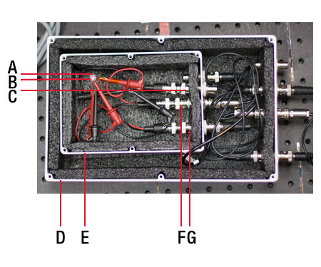
Click to Enlarge
Figure 171L The Nested Metal Box Test Fixture with Covers Removed and FGA10 Installed
Black insulating foam lines the interiors of both boxes.
A: Thermistor; B: FGA10; C: BNC-to-BNC Feedthrough; D: Outer Box; E: Inner Box; F: BNC-to-Triax Feedthrough; G: BNC-to-BNC Feedthrough
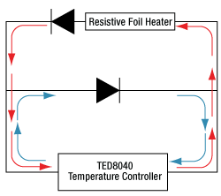
Click to Enlarge
Figure 171N An electrical circuit that included a resistive foil heater, TED8040 temperature controller, and two rectifying diodes controlled current flow through the resistive current heater as described in the text.
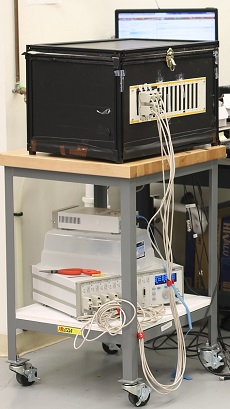
Click to Enlarge
Figure 171M The Test Setup
The custom-built temperature chamber is on the top of the cart, and the temperature control instrumentation that includes the PRO8000 and TED8040 cards is on the cart's lower shelf.
Experimental Setup
The experimental setup was designed to ensure a constant reverse-bias voltage across the photodiode, control the temperature of the detector, block light from reaching the detector, and establish an electrical path between the detector and the Keithley 6487 ammeter that isolated the measured current from extraneous electromagnetic interference (EMI) noise sources. Dark currents for these detectors can be on the order of nA, which made it important to control these conditions to ensure accurate measurements.
The detector enclosure consisted of a pair of nested aluminum metal boxes, which are shown with their covers off in Figure 171L. Only one box would be required to create a light-tight environment for the photodiode, but an outer box was included in the setup to shield the inner box from EMI. The detector was placed inside the inner box, and it was electrically connected to the Keithley 6487 ammeter. The ammeter provided the required 5 V reverse-bias and received the output current signal. The electrical signals between the ammeter and the photodiode were routed through the two boxes using a combination of cables and feedthroughs. The 5 V bias voltage was connected to the photodiode using coax cables and BNC-to-BNC feedthroughs in the walls of both metal boxes. The current signal from the photodiode was connected to the BNC end of a BNC-to-Triax feedthrough integrated into the wall of the inner box. The signal was then routed through the outer box and to the Keithley 6487 using triax cables and a Triax-to-Triax feedthrough in the outer box. Triax cables were used because coax cables are poorly shielded, and using a coax cable to route the signal to the ammeter could introduce noise from EMI sources to the signal read from the detector. As the outer box shields the inner box from EMI, the noise introduced on the signal as it travels from the detector to the BNC-to-Triax feedthrough is mitigated.
Thermistors were used to monitor the temperatures of each photodiode continuously during the experiment. A piece of thermal tape was used to hold the thermistor flush against the TO cans of the FDG50, FGAP71, and the FGA10 during testing. The photosensor of the FDS1010 is mounted on a ceramic substrate, and when it was tested the thermistor was taped to the back of the substrate. The electrical connection between the thermistor and TSP01 temperature logger was performed using BNC cables, BNC-to-BNC bulkhead feedthroughs to route the signal out of the nested boxes, and a custom BNC-to-phono jack cable to connect to the temperature logger.
A custom temperature chamber based on a XE25C9 standard enclosure was used to conduct these tests. It is shown on top of the cart in Figure 171M. The enclosure had a floor and four walls, and insulation was attached to all inner and outer surfaces. A lid for the enclosure was fashioned from a sheet of hardboard bordered with XE25 rails, and insulation was attached to the inner surface of the hardboard. Six resistive foil heaters were affixed to the walls of the XE25C9 enclosure, and they were driven using the PRO8000 fitted with six TED8040 thermoelectric cooler (TEC) controller cards placed on the bottom shelf of the cart in Figure 171M. Each TED8040 was interfaced with a heater and a thermistor installed in the chamber. The reading from the thermistor determined the current sent to drive the heater. The chamber was not actively cooled; cooling was instead performed by withdrawing the current driving the heaters and, as an option, opening the lid of the chamber.
The TED8040 units are designed to be interfaced with TECs, which produce heat when current flows in one direction, and which provide cooling when the current flows in the opposite direction. Because of this, when the enclosure exceeded the setpoint temperature, the TED8040 units in this experimental setup did not cut off the driving current. They instead reversed the current flow in an effort to produce cooling. In contrast to TECs, resistive foil heaters generate heat regardless of the direction of current flowing through them. In order to divert the driving current from the heaters, an electrical circuit, diagrammed in Figure 171N, that included two rectifying diodes was designed and implemented. Rectifying diodes allow current to flow only in one direction. When the temperature reading from the thermistor was lower than the setpoint temperature, current flowed in the direction of the red arrows and through the resistive heater, and heat was generated. When the temperature of the enclosure exceeded the setpoint temperature, the TED8040 controllers reversed the direction of the current, so that it flowed in the direction of the blue arrows. Under this condition, the circuit diverted the current from the heaters and the chamber was allowed to cool.
Experimental Results
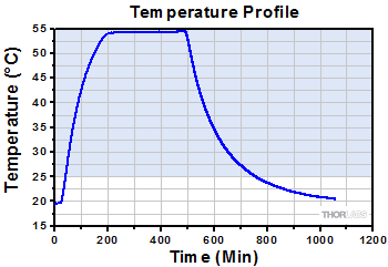
The data curves plotted in Figure 171P are the dark currents measured for the Si-based FDS1010, the Ge-based FDG50, the GaP-based FGAP71, and the InGaAs-based FGA10. Data were acquired continuously while the temperature was between 25 °C and 55 °C (shaded region of Figure 171Q). Figure 171Q is representative of the temperature measured at the photodiode during the experiment. The temperature profile included an initial segment of increasing temperature, followed by a soak that allowed the photodiode to reach the maximum temperature, and concluded with a cool-down. The data plotted in Figure 171P include all dark current measurements measured between 25 °C and 55 °C; current measurements taken at the same temperature, but at different times, overlay one another for each diode.
The data curves plotted in Figure 171P show that the measured dark current magnitudes differed depending on the material composing the photodiode. From lowest to highest:
- GaP-Based Detector FGAP71 (Lowest Dark Current)
- InGaAs-Based Detector FGA10
- Si-Based Detector FDS1010
- Ge-Based Detector FDG50 (Highest Dark Current)
These span approximately 6 orders of magnitude. In all cases, the dark current increased with the temperature of the photodiode, as expected. The individual points on this graph, plotted as diamonds, are the values of the dark current specified for each detector at 25 °C. These points specify a maximum value of dark current at 25 °C; each diode's dark current must be equal to or less than this value at 25 °C, but the dark current may exceed this specification at higher temperatures, as is the case for all but the measured FDS1010 detector.
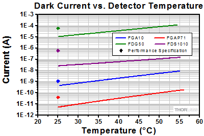
Click to Enlarge
Figure 171P Dark Current Data Measured for Four Unmounted Photodiodes
The discrete data points, plotted as diamonds, are values of the dark current specified for each detector at 25 °C.
Click to Enlarge
Figure 171Q Temperature of a Representative Photodiode Controlled by the Conditions in the Environmental Chamber
Dark current measurements were acquired between 25 °C and 55 °C (indicated by the shaded region) and are plotted in Figure 171P.
Experimental Limitations
Measurements were performed using a single representative of each detector type, as these data were intended to illustrate overall trends. These data should not be taken as specific for a particular diode. The measured dark current is a function of voltage bias, temperature dependence of resistive loads, and other effects. Efforts were made to suppress their influence on these measurements, including using the Keithley 6487 ammeter to provide the required 5 V reverse bias. Using the ammeter removed the need to use a load resisitor, which may exhibit its own temperature dependence. The thermistor was placed as close to the semiconductor sensor as was possible, but it was not placed in direct contact with the sensor. Because of this, there may have been a difference between the measured temperature and the temperature of the semiconductor material. The dark current was measured while the temperature of the environmental chamber was continuously varied. Humidity was not controlled during this experiment.
[1] J. Liu, Photonic Devices. Cambridge University Press, Cambridge, UK, 2005
Noise Equivalent Power (NEP) as a Function of Temperature
Noise Equivalent Power (NEP) was determined as a function of temperature for several unmounted photodetectors. As is described in the following section, NEP is a common metric used to describe the minimum sensitivity of a photodetector. Measurements were taken for silicon (Si), germanium (Ge), gallium phosphide (GaP), and indium gallium arsenide (InGaAs) reverse-biased photodiodes over temperatures from 25 °C to approximately 55 °C.
Noise Equivalent Power
The most general definition of NEP is "the input signal power that results in a signal-to-noise ratio (SNR) of 1 in a 1 Hz output bandwidth." [1] Therefore, in order to determine the NEP, the minimum noise of the photodiode must be determined. When the optical signal is blocked, noise is still present, which is generated by the detector itself. There are two main contributors to photodiode noise: the shot noise due to dark current and thermal noise due to the shunt resistance.
Dark current is a relatively small electric current present in photosensitive devices that flows through the device, including when there is no incident light. More information on the dark current can be found in the "Dark Current as a Function of Temperature" section above. Shot noise is due to the quantized nature of the charge carriers. For the case where there is no light incident on the detector, it can be calculated from the dark current of the detector using the equation [2]

where is is the shot noise, Id is the dark current, q is the electron charge, and fBW is the bandwidth, which will be set to 1 Hz to allow for comparison between different photodiodes.
Thermal, or Johnson, noise is due to the random thermal motion of the charge carriers. Thermal noise will be generated only by the resistive elements of the system. For the photodiode detector, the shunt resistance needs to be considered. Shunt resistance is the resistance of the zero-biased photodiode p-n junction; put another way, it is the inverse of the slope of the I-V curve at the zero-voltage point. Since it is difficult to correctly calculate the slope at the zero crossing, the generally accepted industry practice is to measure the current at V = ±10 mV and then calculate the slope. Then the thermal noise due to the shunt resistance, RSH, can be expressed as:

where it is the thermal noise (expressed as a current), kB is Boltzmann's constant, T is temperature, RSH is shunt resistance, and fBW is the bandwidth.
The total noise, itotal, is the quadrature sum of all noise sources:

Note that this result is the total noise expressed for the current output of the photodiode, while the NEP is expressed in terms of incident optical power. Thus, to compare with the NEP specifications a typical responsivity value,![]() , is chosen for the specified wavelength:
, is chosen for the specified wavelength:

Also, to allow for comparison between different diodes, we set the bandwidth to 1 Hz for the calculation.
Experiment: Dark Current and Shunt Resistance Measurements
NEP was determined over 25 to 55 °C for four representative unpackaged photodiodes: the Si-based FDS1010, the Ge-based FDG50, the GaP-based FGAP71 (previous generation), and the InGaAs-based FGA10.

Click to Enlarge
Figure 171R The nested metal box test fixture with covers removed and FGA10 installed.
Black insulating foam lines the interiors of both boxes.
A: Thermistor; B: FGA10; C: BNC-to-BNC Feedthrough; D: Outer Box; E: Inner Box; F: BNC-to-Triax Feedthrough; G: BNC-to-BNC Feedthrough

Click to Enlarge
Figure 171U An electrical circuit that included a resistive foil heater, TED8040 temperature controller, and two rectifying diodes controlled current flow through the resistive current heater as described in the text.

Click to Enlarge
Figure 171T The Test Setup
The custom-built temperature chamber is on the top of the cart, and the temperature control instrumentation that includes the PRO8000 and TED8040 cards is on the cart's lower shelf.
Experimental Setup
The experimental setup was designed to ensure a constant reverse-bias voltage across the photodiode, control the temperature of the detector, block light from reaching the detector, and establish an electrical path between the detector and the Keithley 6487 ammeter that isolated the measured current from extraneous electromagnetic interference (EMI) noise sources. Dark currents for these detectors can be on the order of nA, which made it important to control these conditions to ensure accurate measurements.
The detector enclosure consisted of a pair of nested aluminum metal boxes, which are shown with their covers off in Figure 171R. Only one box would be required to create a light-tight environment for the photodiode, but an outer box was included in the setup to shield the inner box from EMI. The detector was placed inside the inner box, and it was electrically connected to the Keithley 6487 ammeter. The ammeter provided the required reverse-bias voltage and received the output current signal. The electrical signals between the ammeter and the photodiode were routed through the two boxes using a combination of cables and feedthroughs. The bias voltage was connected to the photodiode using coax cables and BNC-to-BNC feedthroughs in the walls of both metal boxes. The current signal from the photodiode was connected to the BNC end of a BNC-to-Triax feedthrough integrated into the wall of the inner box. The signal was then routed through the outer box and to the Keithley 6487 using triax cables and a Triax-to-Triax feedthrough in the outer box. Triax cables were used because coax cables are poorly shielded, and using a coax cable to route the signal to the ammeter could introduce noise from EMI sources to the signal read from the detector. As the outer box shields the inner box from EMI, the noise introduced on the signal as it travels from the detector to the BNC-to-Triax feedthrough is mitigated.
For dark current measurements, the bias voltage was set to 5 V. In order to calculate the shunt resistance, measurements of the current were made with the bias voltage set to +10 mV and -10 mV.
Thermistors were used to monitor the temperatures of each photodiode continuously during the experiment. A piece of thermal tape was used to hold the thermistor flush against the TO cans of the FDG50, FGAP71, and the FGA10 during testing. The photosensor of the FDS1010 is mounted on a ceramic substrate, and when it was tested the thermistor was taped to the back of the substrate. The electrical connection between the thermistor and TSP01 temperature logger was performed using BNC cables, BNC-to-BNC bulkhead feedthroughs to route the signal out of the nested boxes, and a custom BNC-to-phono jack cable to connect to the temperature logger.
A custom temperature chamber based on a XE25C9 standard enclosure was used to conduct these tests. It is shown on top of the cart in Figure 171U. The enclosure had a floor and four walls, and insulation was attached to all inner and outer surfaces. A lid for the enclosure was fashioned from a sheet of hardboard bordered with XE25 rails, and insulation was attached to the inner surface of the hardboard. Six resistive foil heaters were affixed to the walls of the XE25C9 enclosure, and they were driven using the PRO8000 chassis fitted with six TED8040 thermoelectric cooler (TEC) controller cards placed on the bottom shelf of the cart in Figure 171T. Each TED8040 was interfaced with a heater and a thermistor installed in the chamber. The reading from the thermistor determined the current sent to drive the heater. The chamber was not actively cooled; cooling was instead performed by withdrawing the current driving the heaters and, as an option, opening the lid of the chamber.
The TED8040 units are designed to be interfaced with TECs, which produce heat when current flows in one direction, and which provide cooling when the current flows in the opposite direction. Because of this, when the enclosure exceeded the setpoint temperature, the TED8040 units in this experimental setup did not cut off the driving current. They instead reversed the current flow in an effort to produce cooling. In contrast to TECs, resistive foil heaters generate heat regardless of the direction of current flowing through them. In order to divert the driving current from the heaters, an electrical circuit, diagrammed in Figure 171U, that included two rectifying diodes was designed and implemented. Rectifying diodes allow current to flow only in one direction. When the temperature reading from the thermistor was lower than the setpoint temperature, current flowed in the direction of the red arrows and through the resistive heater, and heat was generated. When the temperature of the enclosure exceeded the setpoint temperature, the TED8040 controllers reversed the direction of the current, so that it flowed in the direction of the blue arrows. Under this condition, the circuit diverted the current from the heaters and the chamber was allowed to cool.
Experimental Results
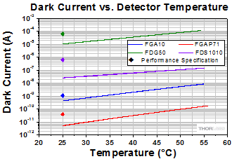
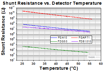
The data curves plotted in Figure 171W are the dark currents measured for the Si-based FDS1010, the Ge-based FDG50, the GaP-based FGAP71, and the InGaAs-based FGA10. Figure 171X shows the calculated shunt resistance values for the same diodes as Figure 171W. Data were acquired continuously while the temperature was between 25 °C and 55 °C (shaded region of Figure 171Z). Figure 171Z is representative of the temperature measured at the photodiode during the experiment. The temperature profile included an initial segment of increasing temperature, followed by a soak that allowed the photodiode to reach the maximum temperature, and concluded with a cool-down. The data plotted in Figures 171W and 171X include all dark current measurements measured between approximately 25 °C and 55 °C; current measurements taken at the same temperature, but at different times, overlay one another for each diode.
As shown in Figure 171X, the shunt resistance for the measured GaP, InGaAs, and Si detectors is relatively large; therefore in many situations it can be ignored. For the Ge-based FDG50 the shunt resistance is relatively low, especially at higher temperatures. For this diode the shunt resistance might need to be considered if there is a high load involved.
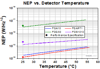
Figure 171Y shows the calculated NEP vs. temperature for each diode. Since the NEP is a function of responsivity, which varies with wavelength, the NEP values are calculated at the peak responsivity value as given in Table 171V.
| Table 171V Responsivity Used for NEP Calculation | |
|---|---|
| FGA10 | 1.05 A/W @ 1550 nm |
| FDG50 | 0.85 A/W @ 1550 nm |
| FGAP71 | 0.12 A/W @ 440 nm |
| FDS1010 | 0.725 A/W @ 970 nm |
The data curves plotted in Figure 171Y show that the calculated NEP magnitudes differed depending on the material composing the photodiode. From lowest to highest:
- GaP-Based Detector FGAP71 (Lowest NEP)
- InGaAs-Based Detector FGA10
- Si-Based Detector FDS1010
- Ge-Based Detector FDG50 (Highest NEP)
These span approximately 6 orders of magnitude. In all cases, the dark current increased with the temperature of the photodiode, as expected. The individual points on this graph, plotted as diamonds, are the values of the dark current specified for each detector at 25 °C. These points specify a maximum value of dark current at 25 °C; each diode's dark current and NEP must be equal to or less than this value at 25 °C, but the dark current and NEP may exceed this specification at higher temperatures.
Click to Enlarge
Figure 171W Dark Current Data Measured for Four Unmounted Photodiodes
The discrete data points, plotted as diamonds, are values of the dark current specified for each detector at 25 °C.
Click to Enlarge
Figure 171X Shunt Resistance Calculated as Described in the Text for Four Unmounted Photodiodes
Click to Enlarge
Figure 171Y NEP Calculated from the Quadrature Sum of Shot Noise and Thermal Noise for Four Unmounted Photodiodes
The discrete data points, plotted as diamonds, are values of the NEP specified for each detector at 25 °C. There is no point for FGA10 since the NEP is not specified at the peak responsivity wavelength.

Click to Enlarge
Figure 171Z Temperature of a Representative Photodiode Controlled by the Conditions in the Environmental Chamber
Dark current measurements were acquired between 25 °C and 55 °C (indicated by the shaded region) and are plotted in Figure 171X.
Experimental Limitations
Measurements were performed using a single representative of each detector type, as these data were intended to illustrate overall trends. These data should not be taken as specific for a particular diode. The measured currents were functions of voltage bias, temperature dependence of resistive loads, and other effects. Efforts were made to suppress their influence on these measurements, including using the Keithley 6487 ammeter to provide the required 5 V reverse bias. Using the ammeter removed the need to use a load resistor, which may exhibit its own temperature dependence. The thermistor was placed as close to the semiconductor sensor as was possible, but it was not placed in direct contact with the sensor. Because of this, there may have been a difference between the measured temperature and the temperature of the semiconductor material. The currents were measured while the temperature of the environmental chamber was continuously varied. Humidity was not controlled during this experiment.
[1] Thorlabs' Noise Equivalent Power White Paper.
[2] Quimby, Richard S. Photonics and Lasers: An Introduction. Wiley-Interscience, Hoboken, NJ, 2006, pp 241-244.
Beam Size and Photodiode Saturation
Click to Enlarge
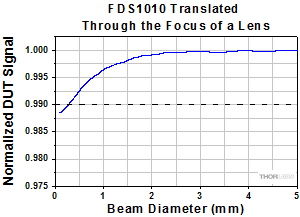
Figure 171AA Normalized change in output current for a fixed incident power as the photodiode Device Under Test (DUT), FDS1010, was translated through the focus of a lens.
We present laboratory measurements showing the effect of beam size on the saturation point of a Thorlabs silicon photodiode. As defined here, saturation is a 1% deviation from the linear response region. As illustrated in Figure 171AA, the photodiode saturated at lower incident power levels as the beam size decreased. Several additional calculations and experiments were performed to verify the cause of the change in saturation was not a function of the power density. These results suggest that users should be cognizant of the beam size when attempting to measure absolute power with a power sensor, such as our S130C photodiode power sensor.
For our experiment, we used the SM1PD1A mounted photodiode, which consists of an FDS1010 photodiode in an SM1-threaded housing. An 830 nm superluminescent diode was used as the light source. A beamsplitter directed 20% of the light to a monitor photodiode while the remainder was transmitted through a focusing lens. Power values were calibrated using an integrating sphere, while the beam size of the focusing beam was calibrated with a beam profiler mounted to a translation stage. After calibration, the beam profiler was replaced with the device under test (DUT), an SM1PD1A at a 0 V bias. The output current was measured with an ammeter to remove the need for a load resistor. We then recorded datasets as the beam diameter was continuously scanned from 0.06 mm to 5 mm while power was held constant, as well as measurements for beam diameters ranging from 1 mm to 5 mm (measured to the 5% clip level) as the incident power was continuously scanned from 0.12 mW to 5 mW.
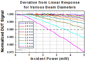
The figures show the results from the measurements. Figure 171AA and Figure 171AB show the deviation from linear response for continuously varying beam diameter at a fixed 1 mW incident power (Figure 171AA) and continuously varying incident power for several beam diameters (Figure 171AB). Figure 171AA shows that for a 1 mW input, the photodiode saturated at beam sizes less than 300 µm. Figure 171AB shows that beam diameters ≥2 mm did not saturate at the power levels investigated.
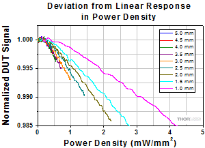
One hypothesis for these results was that local saturation due to a large power density locally depleted or reduced the population of available carriers. In Figure 171AC, we calculated the power density by taking the quotient of the measured power and beam diameter presented in Figure 171AB and plotted the current output as a function of that power density. If the results were due to local saturation, we would have expected that all of the beam diameters would saturate at a single power density; however, this was not the case.
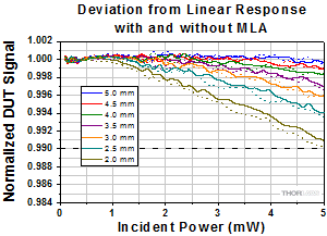
Since the results presented in Figure 171AC coupled the beam size change with a change in optical power density, we performed another experiment to increase the power density incident on the sensor within the same envelope of beam area to see if there was a change in the saturation point. This was done by segmenting the Gaussian beam into an array of beamlets with a microlens array, concentrating the overall optical power into smaller spots within the same Gaussian envelope. This created larger power densities while maintaining a similar electrical path to the sensor leads. Figure 171AD shows the same results as Figure 171AB with the results from the microlens array overlaid as dashed lines. Since the results are nearly identical to the original Gaussian beam for all diameters, the saturation appears to be dependent on the overall beam diameter and independent of the power density. In the complete Lab Facts presentation, we discuss how these results support the theory of Scholze et al. that the change in saturation with beam size is due to a change in the series resistance of the photodiode [1].
Click to Enlarge
Figure 171AB Percent Deviation from the linear response with increasing power for 1 mm - 5 mm beam diameters. The 1% deviation level is indicated with a dashed horizontal line.
Click to Enlarge
Figure 171AC Normalized output current versus power density for 1 mm - 5 mm beam diameters. This shows the saturation effects do not appear to be based on a single power density.
Click to Enlarge
Figure 171AD Normalized output current versus optical power for 2 mm - 5 mm beam diameter with (Dashed Line) and without (Solid Line) the microlens array (MLA) prior to the photodiode.
[1] F. Scholze, R. Klein, R. Muller, Linearity of silicon photodiodes for EUV radiation. 2004 Proc. SPIE 5374 926–34.
Effective Reverse Bias Voltage as a Function of Incident Optical Power
Introduction
The bandwidth (and rise time) of a photodiode is known to be a function of the effective bias across it. Therefore, the effective bias must be tuned in response to the generated photocurrent from the optical power incident on the diode to maintain the desired bandwidth. This lab fact investigates the relationship between the effective reverse bias voltage across a photodiode and the CW optical power incident on it in order to create a reliable model of a biased photodiode.
Circuit Analysis
To begin creating this model, the photodiode circuit shown in Figure 171AF is examined using Ohm’s law and assuming a constant DC voltage source; this yields the equation
Veff = V0 - iPD * (RP + RL).
(1)
The effective bias voltage (Veff) across the photodiode equals the initial voltage from the source (V0) minus the product of the photocurrent (iPD) and the sum of the resistance of the bias module's resistor (RP) and the load resistor (RL).
To find how Veff changes with respect to the incident optical power (P), iPD is replaced in Equation 1 with its definition as the product of the wavelength-dependent responsivity [ℜ(λ)] of the photodiode and P:
iPD = ℜ(λ) * P.
(2)
Using Ohm’s law on the load resistor such that iPD = VL / RL, Equation 2 was rewritten to solve for ℜ(λ):
ℜ(λ) = VL / (P * RL ).
(3)
Assuming that the voltage drop across the load resistor (VL) is linear with respect to increasing P, the ratio of the change in VL and P can be established as the ratio:
m = Δ VL / Δ P.
(4)
These equations can be combined to form:
Veff = V0 - (m / RL) * P * (RP + RL).
(5)
The ratio m can be calculated from empirical measurements of VL and P for each photodiode, allowing this equation to be used as a model for how Veff changes with respect to P.
Experiment
An experiment was developed to measure the change in VL with respect to changes in P. Output from a fiber-coupled laser diode was collimated, passed through a neutral density filter, and then focused onto the Device Under Test (DUT) via an off-axis parabolic mirror. A photograph of the setup used can be seen in Figure 171AE. Neutral density filters with a range of optical densities were used to vary the power incident on the photodiode. For each photodiode used, the distance between the sensor surface and focusing mirror was adjusted so that the spot size was approximately half the size of each photodiodes’ detector area. An oscilloscope was used to measure V0, VL, and the sum Veff + VL. A multimeter was used to measure the effective bias directly.
Results
VL was plotted against P for each DUT; an example of the results for the silicon photodiode can be seen in Figure 171AG. A linear trend line was created for each data set, and the slope of that line corresponds to m in Equation 4. This value can be used in Equation 5 to calculate the effective bias voltage. Then, Veff can be plotted with respect to the incident power and compared to the measured values from the oscilloscope. These results are shown in the three graphs displayed in Figures 171AH, 171AJ, and 171AK. The model was found to be consistent with measured experimental results, which showed that Veff decreases as P increases (with V0, RP, and RL held constant). This effect is significant, because the voltage set at the voltage source is not necessarily the bias voltage applied to the photodiode; one must account for resistive components within the circuit to calculate the effective bias voltage applied across the photodiode.
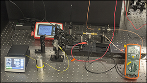 Click to Enlarge
Figure 171AE: This setup was used in the experiment in order to verify our model of the effective voltage across the photodiode.
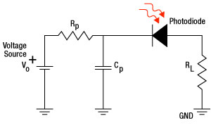
Click to Enlarge
Figure 171AF: Circuit Diagram of Biased Photodiode
_Plot_G1-300.gif)
Click to Enlarge
Figure 171AG: A single voltage vs. incident power graph used to find m for the final model, Equation 5.
_Power_Plot_G1-300.gif)
Click to Enlarge
Figure 171AK Measured Effective Bias Values for
SM05PD6A with Their Modeled Values
_Power_Plot_G1-300.gif)
Click to Enlarge
Figure 171AJ Measured Effective Bias Values for
SM05PD5A with Their Modeled Values
_Power_Plot_G1-300.gif)
Click to Enlarge
Figure 171AH Measured Effective Bias Values for
SM05PD1A with Their Modeled Values
About Our Lab Facts
Our application engineers live the experience of our customers by conducting experiments in Alex’s personal lab. Here, they gain a greater understanding of our products’ performance across a range of application spaces. Their results can be found throughout our website on associated product pages in Lab Facts tabs. Experiments are used to compare performance with theory and explore the benefits and drawbacks of using similar products in unique setups, in an attempt to understand the intricacies and practical limitations of our products. In all cases, the theory, procedure, and results are provided to assist with your buying decisions.
Pulsed Laser Emission: Power and Energy Calculations
Determining whether emission from a pulsed laser is compatible with a device or application can require referencing parameters that are not supplied by the laser's manufacturer. When this is the case, the necessary parameters can typically be calculated from the available information. Calculating peak pulse power, average power, pulse energy, and related parameters can be necessary to achieve desired outcomes including:
- Protecting biological samples from harm.
- Measuring the pulsed laser emission without damaging photodetectors and other sensors.
- Exciting fluorescence and non-linear effects in materials.
Pulsed laser radiation parameters are illustrated in Figure 170A and described in Table 170B. For quick reference, a list of equations is provided below. The document available for download provides this information, as well as an introduction to pulsed laser emission, an overview of relationships among the different parameters, and guidance for applying the calculations.
|
Equations: |
||||
 |
and |  |
||
 |
||||
 |
||||
 |
||||
Peak power and average power calculated from each other: |
||||
 |
and |  |
||
| Peak power calculated from average power and duty cycle*: | ||||
 |
*Duty cycle ( ) is the fraction of time during which there is laser pulse emission. ) is the fraction of time during which there is laser pulse emission. |
|||
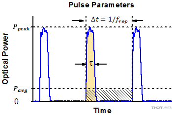
Click to Enlarge
Figure 170A Parameters used to describe pulsed laser emission are indicated in this plot and described in Table 170B. Pulse energy (E) is the shaded area under the pulse curve. Pulse energy is, equivalently, the area of the diagonally hashed region.
| Table 170B Pulse Parameters | |||||
|---|---|---|---|---|---|
| Parameter | Symbol | Units | Description | ||
| Pulse Energy | E | Joules [J] | A measure of one pulse's total emission, which is the only light emitted by the laser over the entire period. The pulse energy equals the shaded area, which is equivalent to the area covered by diagonal hash marks. | ||
| Period | Δt | Seconds [s] | The amount of time between the start of one pulse and the start of the next. | ||
| Average Power | Pavg | Watts [W] | The height on the optical power axis, if the energy emitted by the pulse were uniformly spread over the entire period. | ||
| Instantaneous Power | P | Watts [W] | The optical power at a single, specific point in time. | ||
| Peak Power | Ppeak | Watts [W] | The maximum instantaneous optical power output by the laser. | ||
| Pulse Width |  |
Seconds [s] | A measure of the time between the beginning and end of the pulse, typically based on the full width half maximum (FWHM) of the pulse shape. Also called pulse duration. | ||
| Repetition Rate | frep | Hertz [Hz] | The frequency with which pulses are emitted. Equal to the reciprocal of the period. | ||
Example Calculation:
Is it safe to use a detector with a specified maximum peak optical input power of 75 mW to measure the following pulsed laser emission?
- Average Power: 1 mW
- Repetition Rate: 85 MHz
- Pulse Width: 10 fs
The energy per pulse:

seems low, but the peak pulse power is:

It is not safe to use the detector to measure this pulsed laser emission, since the peak power of the pulses is >5 orders of magnitude higher than the detector's maximum peak optical input power.
| Posted Comments: | |
Michael Matthews
(posted 2025-05-06 19:26:37.8) I've used many of the SM05PD4A recently, and in every case the active area is not coaxial with the SM05 threads. It can be off by a large fraction of the 1mm detector. This results in significant beam walk-off and signal loss when the detector is rotated to adjust focus.
I've occasionally been able to 3D print a plastic cylindrical spacer and use it to force recenter (after popping off the black front cover). That does help sometimes, but not always. It's likely my 3D printer isn't good enough, and that I should switch to aluminum.
It would be nice if you could redesign for better center.
Best,
Mike. ksosnowski
(posted 2025-05-12 10:00:05.0) Hello Michael, thanks for reaching out to us. Unfortunately, with the small size of this detector this is expected. We often use translation mounts like
ST1XY-A to adjust the beam position over the sensor area. I have reached out directly to discuss your application in further detail. Ahsan Uddin
(posted 2024-09-27 15:17:10.92) Could you provide a Large Area Mounted Silicon Photodiode, 350 - 1100 nm, with Anode as central contact and Cathode as outer contact to a triax connector? jpolaris
(posted 2024-09-28 12:37:18.0) Thank you for contacting Thorlabs. Requests for customizations such as this can be made by emailing us at techsupport@thorlabs.com. I have reached out to you directly to discuss the feasibility of this request. user
(posted 2024-08-10 18:37:24.807) Hi, I am working with the SM1PD2A photodiode and would like to know if I am correctly applying the reverse bias. I have a voltage supply that supplies 0-5V to the photodiode through the RC circuit presented in the Spec Sheet and a picoammeter to measure the photodiode's current output. I tried to measure the dark current with this setup, but the current values I was reading were in the magnitude of nanoamps, which didn't add up to the maximum dark current, 1-micron amp, provided on the Spec Sheet, even at 5V. The female BNC port of the picoammeter had a resistance of 16M Ohms between the core and outer shell, and I was wondering if that could've been an issue when measuring current. ksosnowski
(posted 2024-08-19 10:58:48.0) Thank you for reaching out to us. This level of dark current sounds normal for SM1PD2A. Our specification guarantees the dark current will be less than or equal to 1uA at 5V bias. Often we will use a 1MOhm oscilloscope to check the dark current, which provides mV scale readings for nA scale currents. It is also fine to use an ammeter for this purpose. I have reached out directly to discuss this application further. Katherine Han
(posted 2024-05-20 11:40:45.14) Hi, can you provide the IV curve for this photodiode at a specific illumination? ksosnowski
(posted 2024-05-28 04:22:10.0) Hello Katherine,
Thanks for reaching out to Thorlabs. The photodiodes will act as a linear current source when below saturation so the output voltage will be determined by the load resistor used for measurement. We do not recommend operating the photodiode past the saturation point as the measurement is not reliable and photons can only convert to heat instead of electric current in this condition. InGaAs saturates at a fairly low photovoltaic level around 300mV depending on the exact photodiode, and typically a bias voltage is applied to directly extend the linear photoconductive range of output. The measurement load should be low enough so that the expected photocurrent will not exceed the biased or photovoltaic levels when considering Ohm's law for the measured voltage. Yoshinori Matsumoto
(posted 2023-05-25 11:31:56.55) Looking at the drawing of SM05PD2B, there is a set screw on the SMA connector side, can it be used to fix it to the chassis? cdolbashian
(posted 2023-06-01 02:21:32.0) Thank you for reaching out to us with your inquiry. I am not sure which "set screw" you are speaking of. I have reached out to you directly to clarify this. There is a locking nut on the SMA connector though this is mainly for locking the SMA cable in place. If you want to fix this to a chassis, I would recommend using the SM05 threadings on the outer, black-anodized, body of the component. Osman Levent Şavkay
(posted 2023-05-17 22:25:32.097) we have bought SM1PD1A Si Photodiode and AMP110 transimpedance amplifier. We applied the circuit diagram shown on the document of SM1PD1A and obtain the voltage output correctly. Now we want to use the AMP110 with SM1PD1A, please reccomend us a connection diagram for a setup using both products together.
Best Regards,
Levent Şavkay dpossin
(posted 2023-05-17 09:58:52.0) Dear Tolga,
Thank you for your feedback. I am reaching out to you in order to provide the requested support. Ao Teng
(posted 2022-01-30 23:38:49.973) Hello, I'd like to inquire about how to fix this product. Do you have any products that can fix SM05PD3A?
Thank you! cdolbashian
(posted 2025-01-22 03:39:17.0) Thank you for reaching out to us with this inquiry. We are happy to process a repair for you via our RMA team. I have reached out to you directly to facilitate this. Dirk Hönig
(posted 2021-10-15 10:52:27.517) Hello, we have purchased the SM1PD2A and found that the case is NOT connected to the BNC, opposite to the drawing in the online catalog. This fits to the fact that the BNC is an isolated one.
I guess it's a copy/paste typo from the smaller SM05 diodes ?
To get a low-noise measurement done with our TIA, we had to remove a bit of the case anodizing to connect the case to the shielding of a shielded double wire cable (microphone cable).
What's missing in the data is a responsivity temperature coeff vs. wavelength graph (or at least UV, VIS, NIR regime values). In the Lab Facts section, you show extensive temperature measurements, but not on spectral responsivity, did I miss it somewhere?
Thanks,
Dirk cdolbashian
(posted 2021-11-08 04:57:25.0) Thank you for reaching out to us with this feedback Dirk. I have reached out to you directly to discuss your application. Regarding the "case", this is referring to the housing of the PD itself, rather than the anodized housing in which the photodiode is mounted within. For your specific application, we found that with a different cable (shielded 2-wire microphone cable), stripping of some of the anodized layer, and connecting the mounted housing to the alternative cable's ground, we were able to see a notable reduction in the ambient noise in this device. I have logged this internally as a potential improvement/alternate item for future releases. Claudia Ruiz
(posted 2021-09-09 10:50:41.003) Hello what is the SM05PD1A FOV?
Thanks cdolbashian
(posted 2021-09-20 01:42:39.0) Thank you for contacting Thorlabs with this inquiry. The half-angle FOV for the component diode (FDS100) is 61 degrees from the center of the active area, measured from the normal. Since the housing obscures the FOV, the mounted version (SM05PD1A) has a half-angle FOV of approximately 39 degrees. user
(posted 2021-09-04 18:09:33.997) Could you please tell me the maximum input power (damage threshold) of SM05PD2A? Thank you very much! cdolbashian
(posted 2021-09-20 01:32:53.0) Thank you for contacting us at Thorlabs! The maximum input power depends directly on the responsivity, bias voltage, and termination of your device. Applying a bias voltage will determine the max output voltage measurable on your device, and thus the electrical saturation. While operating below the bias voltage, your laser's wavelength will determine the conversion of optical power to a photocurrent. We have a nice investigation of these behaviors here: https://www.thorlabs.com/newgrouppage9.cfm?objectgroup_id=10741
I have contacted you directly with more information. Niklas Papathanasiou
(posted 2021-08-19 03:21:04.89) Hi,
is it possible to get an SM05PD with a photodiode socket STO5P für TO5 photodiodes?
I want to use my own (calibrate reference) photodiodes within the cage system at a fixed position. Or should I assaemble something on my own?
best regards
Niklas cdolbashian
(posted 2021-08-26 03:43:44.0) Thank you for reaching out to us here with this feedback Niklas. After discussing this with you directly, I have understood that you are looking for something similar to our strain-relief cables (used for laser diodes), but wired for photodiodes but with a PD socket. Unfortunately, this is not something we have at this time. We are, however, always hungry for feedback, and appreciate the suggestion! Aadil Raza
(posted 2021-07-09 15:30:38.32) Dear Sir
May I know the modulation bandwidth of
SM05PD6A - Large Area Mounted Germanium Photodiode, 800-1800 nm, Cathode Grounded.
Can we use it for optical communication applications? cdolbashian
(posted 2021-07-13 08:34:50.0) Thank you for contacting Thorlabs! In general these devices can be used however you want to, assuming the functionality fits your needs. The particular photodiode you are looking at will have a rise time of 600ns and therefore can respond to a 10-90 modulated signal having a ~583kHz frequency (.35/rise time). I have emailed you directly to discuss your application. Claudia Ruiz
(posted 2020-07-29 11:11:41.077) Hello, Could you please provide the junction capacitance of SM05PD1A at 0V? thank youin advance, Claudia YLohia
(posted 2020-07-29 11:11:56.0) Hello Claudia, thank you for contacting Thorlabs. The corresponding component-level photodiode for these mounted detectors are given on the Specs on this page. The photodiode for the SM05PD1A is the FDS100: https://www.thorlabs.com/newgrouppage9.cfm?objectgroup_id=285&pn=FDS100. Clicking on the blue "info" icon on this link next to the part number brings up additional specs, which contains a Capacitance vs. Bias Voltage plot. We will make this more visible on this product page. Youngki Kim
(posted 2020-07-23 01:59:06.89) Is the photodiode compatible with other multimeters (not from Thorlab, for example, from Keysight, Newport...)? YLohia
(posted 2020-07-23 10:55:59.0) Thank you for contacting Thorlabs. Yes, these photodiodes are compatible with 3rd party multimeters and oscilloscopes. Andrey Kuznetsov
(posted 2020-06-11 16:30:36.16) Could Thorlabs offer standard product or provide quote for FD05D and FD10D devices mounted in SM05 housing like the SM05PD2A for example? asundararaj
(posted 2020-06-12 08:29:51.0) Thank you for contacting Thorlabs. Quotes can be requested by clicking the Request Quote button or by emailing techsupport@thorlabs.com. I have contacted you directly regarding the custom offering. giora chrmoni
(posted 2020-05-05 18:10:30.403) hou i connect to FIBER OPTIC SC/apc ? YLohia
(posted 2020-05-06 10:33:39.0) Thank you for contacting Thorlabs. You can use the SM05SC adapter with the SM05M05 tube to connect an SC/APC fiber to the SM05PD4A. Please note that the fiber tip will need to be positioned relatively close to the sensor since the SM05SC will not correct for the tilt from the angled connector. user
(posted 2019-11-29 06:19:27.34) Hello,
we need to know the electrical impedance of the SM1PD1A Photodiode (50 Ohm ?). We bought three of them to measured a pulsed signal (up to 10MHz).
Thanks!
Petra asundararaj
(posted 2019-12-05 01:52:53.0) Thank you for contacting Thorlabs. The SM1PD1A is a photodiode mounted in an BNC mount and does not have any external circuitry. For maximum bandwidth, we recommend using a 50 Ω coaxial cable with a 50 Ω terminating resistor at the opposite end of the cable. This will minimize ringing by matching the cable with its characteristic impedance. Pawel Czuma
(posted 2019-10-14 06:37:17.177) Dear Sir/Madam,
I am looking for detector for measurement pulse-to-pulse stability of femtosecond amplified laser (1035nm, 515nm, 257nm) with pulse duration of 100fs at 50kHz plus oscillator 1035nm/73MHz/70fs. Please choose me appropriate avalanche/amplified photo-diode with description of maximum input average/peak pulse power, that will damage the detector
Best Regards,
Eng. Pawel Czuma, PhD YLohia
(posted 2019-10-15 09:35:31.0) Hello Pawel, thank you for contacting Thorlabs. Avalanche/amplified photodiodes do not have fast enough rise times to directly measure femtosecond pulses. You would have to use an autocorrelator such as our FSAC to measure such pulses. g.d.j.sasbrink
(posted 2017-01-09 06:10:55.967) Dear Thorlabs,
I'm looking for a mounted, calibrated PD. The FDS100-CAL seems to be a suitable option. We do need the PD to be mounted however. The SM05PD1A seems to be the corresponding mounted product. I see that it is possible to obtain the SM05PD1A with a calibrated PD (as a custom product). What would be the price?
Thanks. tfrisch
(posted 2017-01-09 10:42:02.0) Hello, thank you for contacting Thorlabs. We have been able to offer mounted calibrated photodiodes in the past. I will contact you directly about your needs. bcaplins
(posted 2016-03-11 10:58:17.647) I am planning to detect small signal from a 1 KHz laser with these PD's. I will be using a SRS 570 current amp which has a floating input. I was curious to know if there is any benefit to the cathode grounded vs anode grounded version? Seems like it shouldn't matter to me. besembeson
(posted 2016-03-11 04:08:10.0) Response from Bweh at Thorlabs USA: Yes it shouldn't really matter. 1982ariel
(posted 2015-01-15 15:28:34.47) ThoeLabs hello,
Please advise damage threshold on all your Si, GaAs,Ge and other detectors.
Thank you
Ariel myanakas
(posted 2015-02-09 08:41:46.0) Response from Mike at Thorlabs: We do not currently have damage threshold specifications for these photodiodes. We have contacted you directly to discuss you application. robertmeissner
(posted 2014-11-20 16:11:23.863) Dear Thorlabs, I want to measure the power of my laser with a SM1PD2A attached to an oscilloscope. I read that the maximum power is roughly a couple of mW. What is the maximum measurable voltage/current of this device?
Could you tell me more about the I-V curve as well? Is a bias-voltage needed and if so, which voltage is needed? jlow
(posted 2014-11-25 10:51:12.0) Response from Jeremy at Thorlabs: The maximum reverse bias voltage is 5V. A reverse bias is not necessary but it will result in faster response and better linearity. We will contact you directly to discuss more about your application and provide more details. holmiumht125
(posted 2014-10-03 12:53:33.787) Dear Thorlabs, I would like to use the photodiode with an oscilloscope to measure the energy of laser pulse of ~10ns.
For the same laser pulse, the signal looks very different for oscilloscope impedance of 50 Ohms and 1 MOhms.
Which 1 should be used to measure energy of laser pulse?
And how should be be calculated (min/max value, area under graph, etc)?
Thanks. jlow
(posted 2014-10-03 02:16:45.0) Response from Jeremy at Thorlabs: These mounted photodiode are current source and you will not get a good signal for your application by using the oscilloscope with 1MOhm impedance. The 50Ohm input would be much better. You will also want to make sure to properly bias the photodiodes. For calculating the pulse energy, you will need a calibrated sensor which these mounted photodiodes are not. I will contact you directly to discuss more about your application and suggest something appropriate. david.lee
(posted 2014-03-10 17:52:25.753) Dear Thorlabs team,
Do you have any information regarding the change in responsivity of the SM1PD1B photodiode as a function of temperature. I am interested in data for the temperature range 0C - 40C.
Thank you. jlow
(posted 2014-03-10 04:17:47.0) Response from Jeremy at Thorlabs: The responsivity change will be more significant on the extreme ends of the responsivity curve. I will contact you directly to provide a typical graph for this. th6187
(posted 2013-11-19 11:17:21.65) Dear Thorlabs team, could you tell me damage threshold of the SM1PD1A and/or the recommended power range which this photodiode is suitable for? Thank you. jlow
(posted 2013-11-21 10:59:27.0) Response from Jeremy at Thorlabs: We recommend that the input power to be at most a few mW to make sure that the detector is not being saturated or operating in the nonlinear regime. As for the damage threshold, you would want to keep the detector output current to be <10mA. ch605852
(posted 2013-10-27 13:37:37.607) Is there any V-I characteristics of the diode itself? Specifically I am looking for information about output voltage respect to reverse bias and incident power. Thanks. jlow
(posted 2013-10-29 14:19:00.0) Response from Jeremy at Thorlabs: The output current should be linear with respect to the incident power up until a few mW. I will get in contact with you directly to discuss about this. th6187
(posted 2013-07-15 14:30:03.043) Dear Thorlabs team,
do you have any information or data concerning a possible polarization dependence of the SM1PD1A? If so, I would be grateful if you could send it to me.
Thanks, SR jlow
(posted 2013-07-16 11:40:00.0) Response from Jeremy at Thorlabs: The polarization effects depends on the angle of incidence (AOI). At 0° AOI, both s and p-polarization should yield the same result. I will get in contact with you to discuss about this further. jlow
(posted 2012-07-31 17:44:00.0) A response from Jeremy at Thorlabs: Thank you very much for your feedback. I have forwarded this to our engineering group and we will look into getting this implemented. acable
(posted 2012-07-31 09:41:16.0) I have modified your SM05PD1A sensor, the back end was to large to fit through a SM05 lens tube, by turning down the diameter of the unthreaded portion of the housing diameter to just below 0.450" i was able to get the parts to fit together nicely. Please consider reducing the diameter on all the detector housings so they fit into your standard lens tubes. tcohen
(posted 2012-05-23 19:58:00.0) Response from Tim at Thorlabs: Thank you for your feedback! We have found a couple errors on the web presentation that may have caused some confusion. We are confirming these values, will fix the errors and will clear up any ambiguity. Thank you for helping us improve our website! user
(posted 2012-05-18 16:26:39.0) There seems to be an error that has effected all you detector pages, looking at the NEP for the 0.8 mm^2 and 13 mm^2 area SI detectors in their various forms, the NEP values are different on the bare diode, package diodes from this page, and the biased detector pacakges. Please confirm the numbers, perhaps i am missing something and your packaging effects the NEP more than expected. jvigroux
(posted 2011-12-02 12:09:00.0) A response from Julien at Thorlabs: Thank you for your question. The cathode is connected to the housing and to the outer electrode of the BNC plug strikovski
(posted 2011-11-30 09:15:26.0) Please, clarify the electrical connection of the SM1PD2A: is Cathode directly connected to the diode case, and to BNC connector outer electrode?
Sorry, that is not clear from your Spec Sheet.
Thank you beforehand.
Mikhail Strikovski
strikovski@neocera.com
NEOCERA LLC, USA bdada
(posted 2011-10-17 14:07:00.0) Response from Buki at Thorlabs:
Thank you for your feedback. We will add more detailed drawings to our website soon. Please contact TechSupport@thorlabs.com for further questions. michael.vilcheck
(posted 2011-10-12 15:04:48.0) The product drawings do not locate the detector plane. The drawing for the photodiode locates the plane relative to the front window, but the location of the photodiode within the delrin SM05 housing is not given. Could you please provide a drawing that locates the detector plane. Even better would be a solid model.
Thank you,
Michael tor
(posted 2010-11-10 17:00:23.0) Response to ericsmoll from Tor at Thorlabs: Thank you for your interest in the SM1PD1A. I will send a plot of the typical capacitance per unit area as function of reverse bias voltage. Our Electronics Department indicates that the capacitance is 1500pF for 0V and settles down to 300pF for 10V. ericsmoll
(posted 2010-11-09 13:13:06.0) Do you have a plot of SM1PD1A capacitance as a function of reverse bias? lmorgus
(posted 2010-01-07 10:14:09.0) Response from Laurie at Thorlabs to the anonymous poster: We are please to hear that you find the drawings on our overview tab helpful. We have enlarged those images to make the text easier to read. We hope these will be beneficial to you, and thank you for helping us to improve our website. apalmentieri
(posted 2010-01-06 16:51:03.0) A response from Adam at Thorlabs: You are correct, the text is rather small. We will enlarge the drawings on the overview tab to make them easier to read. user
(posted 2010-01-06 16:18:14.0) The drawings on the Overview tab are great as quick reference aids but i cant read the text, can you please enlarge. Tyler
(posted 2008-04-14 16:58:02.0) A response from Tyler at Thorlabs to tehola: I believe the best option Thorlabs can offer you with our stock parts to mount a TO-18 can photodiode on the optical axis of an SM05 lens tube is to use an S1LEDM mount in conjunction with an SM1A1. Note that unlike the mounted photodiodes that we sell, the S1LEDM is made from anodized aluminum and as a result the TO-18 can will not be insulated from the lens tube. I will forward your request to our design engineers. Hopefully, this will result in the development of a new product. Thank you for letting us know what kinds of tools you need for your lab. tehola
(posted 2008-04-14 03:21:16.0) Dear Sirs,
It would be great, if you had such a product that could be used to mount a separate photodiode for example in TO-18 can to SM05 tube so that it is centered. Is it possible to get such a device at the moment from you and in what cost?
-TH- |
The following table lists Thorlabs' selection of photodiodes, photoconductive, and pyroelectric detectors. Item numbers in the same row contain the same detector element.

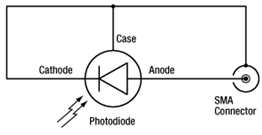
Figure G1.1 Circuit Diagram of Cathode-Grounded Photodiodes
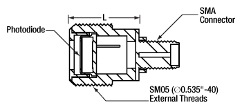
Please click on the red document icons (
| Item #a | Detector Infob |
Rise/Fall Time (Typ.)c |
Active Area (Dimensions) |
NEP (W/Hz1/2) |
Dark Current |
Spectral Range (nm) |
Material | Junction Capacitance (Typ.) |
Reverse Bias Voltage (Max) |
Responsivity Plots |
|---|---|---|---|---|---|---|---|---|---|---|
| SM05PD2A | FDS010 | 1 ns / 1 ns @ 10 V | 0.8 mm2 (Ø1.0 mm)d | 5.0 x 10⁻¹⁴ | 0.3 nA @ 10 V | 200 - 1100e | Si | 6 pF @ 10 V | 25 V | |
| SM05PD8A | FDBS22 | 25 ns / 29 ns @ 650 nm, 10 V |
4.0 mm2 (2.0 mm x 2.0 mm) |
7.1 x 10⁻¹⁵ | 1 nA (Max) @ 10 V | 240 - 1170 | B-Si | 13 pF @ 10 V | 20 V | |
| SM05PD9A | FDBS11 | 15 ns / 19 ns @ 650 nm, 10 V |
1.0 mm2 (1.0 mm x 1.0 mm) |
5.8 x 10⁻¹⁵ | 250 pA (Max) @ 10 V | 240 - 1170 | B-Si | 4 pF @ 10 V | 10 V | |
| SM05PD3Af | FD11A | 15 ns / 15 nsg @ 650 nm, 10 V |
1.21 mm2 (1.1 mm x 1.1 mm) |
4.2 x 10⁻¹⁵ | 20 pA (Typ.) @ 10 V 100 pA (Max) @ 10 V |
320 - 1100 | Si | 140 pF @ 0 V | 30 V | |
| SM05PD1A | FDS100 | 10 ns / 10 nsg @ 632 nm, 20 V |
13 mm2 (3.6 mm x 3.6 mm) |
1.2 x 10⁻¹⁴ | 1.0 nA (Typ.) @ 20 V 20 nA (Max) @ 20 V |
350 - 1100 | Si | 24 pF @ 20 V | 25 V | |
| SM05PD10A | FGA015 | 0.3 ns / 0.3 ns @ 5 V | 0.018 mm2 (Ø0.15 mm) | 1.3 x 10⁻¹⁴ | 0.5 nA @ 5 V | 800 - 1700 | InGaAs | 1.5 pF @ 5 V | 20 V | |
| SM05PD5A | FGA21 | 25 ns / 25 ns @ 3 V | 3.1 mm2 (Ø2.0 mm) | 6.0 x 10⁻¹⁴ | 50 nA @ 1 V | 800 - 1700 | InGaAs | 100 pF @ 3 V | 3 V | |
| SM05PD6A | FDG03 | 600 ns / 600 ns @ 3 V |
7.1 mm2 (Ø3.0 mm) | 2.6 x 10⁻¹² | 4.0 µA (Max) @ 1 V | 800 - 1800 | Ge | 6 nF @ 1 V 4.5 nF @ 3 V |
3 V | |
| SM05PD4A | FGA10 | 10 ns / 10 ns @ 5 V | 0.8 mm2 (Ø1.0 mm) | 2.5 x 10⁻¹⁴ | 1.1 nA @ 5 V | 900 - 1700 | InGaAs | 80 pF @ 5 V | 5 V |

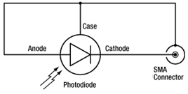
Figure G2.1 Circuit Diagram of Anode-Grounded Photodiodes

Please click on the red document icons (
| Item # | Detector Infoa |
Rise/Fall Time (Typ.)b |
Active Area (Dimensions) |
NEP (W/Hz1/2)c |
Dark Current |
Spectral Range (nm) |
Material | Junction Capacitance (Typ.) |
Reverse Bias Voltage (Max) |
Responsivity Plot |
|---|---|---|---|---|---|---|---|---|---|---|
| SM05PD2B | FDS010 | 1 ns / 1 ns @ 830 nm, 10 V |
0.8 mm2 (Ø1.0 mm) | 5.0 x 10⁻¹⁴ | 0.3 nA (Typ.) @ 10 V | 200 - 1100d | Si | 6 pF @ 10 V | 25 V | |
| SM05PD1B | FDS100 | 10 ns / 10 nse @ 632 nm, 20 V |
13 mm2 (3.6 x 3.6 mm) | 1.2 x 10⁻¹⁴ | 1.0 nA (Typ.) @ 20 V 20 nA (Max) @ 20 V |
350 - 1100 | Si | 24 pF @ 20 V |

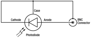
Figure G3.1 Circuit Diagram of Cathode-Grounded Photodiodes
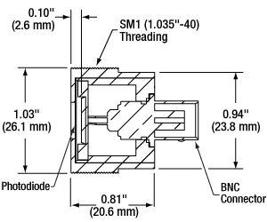
Unless otherwise noted, all measurements are performed at 25 °C.
| Item # | Detector Infoa |
Rise/Fall Time (Typ.)b,c |
Active Area (Dimensions) |
NEP (W/Hz1/2) |
Dark Current |
Spectral Range (nm) |
Material | Junction Capacitance (Typ.) |
Reverse Bias Voltage (Max) |
Responsivity Plots |
|---|---|---|---|---|---|---|---|---|---|---|
| SM1PD2A | - | 450 ns / 450 ns @ 650 nm, 5 V |
Behind Ø9 mm Clear Aperture |
1.0 µA (Max) @ 5 V |
Si | 1.75 nF @ 0 V | 5 V | |||
| SM1PD1A | FDS1010 | 65 ns @ 632 nm, 5 V |
600 nA (Max) @ 5 V |
Si | 375 pF @ 5 V | 25 V |

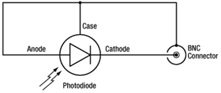
Figure G4.1 Circuit Diagram of Anode-Grounded Photodiodes

| Item # | Detector Infoa |
Rise/Fall Time (Typ.)b,c |
Active Area (Dimensions) |
NEP (W/Hz1/2) |
Dark Current |
Spectral Range (nm) |
Material | Junction Capacitance (Typ.) |
Reverse Bias Voltage (Max) |
Responsivity Plots |
|---|---|---|---|---|---|---|---|---|---|---|
| SM1PD1B | FDS1010 | 65 ns @ 632 nm, 5 V |
10 mm x 10 mm Behind Ø9 mm Clear Aperture |
2.07 x 10⁻¹³ | 600 nA (Max) @ 5 V | 350 - 1100 | Si | 375 pF @ 5 V | 25 V |

| Specifications | |
|---|---|
| Bias Voltage | -25 to + 25 V |
| Cutoff Frequencya | 350 MHz |
| Photodiode Input Connector | Female BNC |
| Output Connector | Female SMA |
| DC Input Connector | 2.5 mm Phono Jack (Cable Included) |
| Housing Dimensions | 2.48" x 1.40" x 0.80" (63.0 mm x 35.6 mm x 20.3 mm) |
| Operating Temperature | 0 to 40 °C |
| Storage Temperature | 0 to 40 °C |
- Module for DC Biasing Our Mounted Photodiodes
- Delrin®* Housing Isolates Connectors and Bias Source
- Post Mountable via Bottom-Located 8-32 and M4 Taps
The PBM42 Bias Module allows a DC bias voltage from a user-supplied, external source to be applied to photodiodes. Designed for use with our mounted photodiodes, the module can accept an input bias voltage from -25 to +25 V from a user-supplied source and has a maximum bandwidth of 350 MHz (dependent on the photodiode).
The input side of the bias module has a BNC connector that can be connected to any of our mounted photodiodes equipped with the same connector by using a BNC cable or T3533 BNC adapter. Alternatively, the input side can be connected to any of our mounted photodiodes with SMA connectors by using an SMA-to-BNC cable or T4001 SMA-to-BNC adapter.
The bias module has an SMA connector on the output side and a 2.5 mm phono jack for the DC voltage input. A 72"-long cable with a 2.5 mm phono plug on one end and bare wires on the other is included with the module. Please note that the photodiode should be operated with a reverse bias. Forward biasing the photodiode can cause damage. For cathode-grounded photodiodes, the tip of the phono plug must be positive. For anode-grounded photodiodes, the tip of the phono plug must be negative. We recommend using a low-noise power supply with the module. For grounding and reverse bias voltage information on all our mounted photodiodes, please see the tables above.
For best frequency performance, the output of the bias module should be terminated with a 50 Ω cable and a 50 Ω impedance device or terminator, such as our T4119. For flexibility in output voltage, the VT2 variable terminator can also be used.
To ensure electrical isolation of the connectors and to protect the photodiode, the compact housing of the PBM42 is constructed from Delrin. Additionally, the housing offers one 8-32-tapped hole and one M4-tapped hole for mounting on our Ø1/2" posts, as shown on the Overview tab.
For more information, please see the full presentation on the PBM42 Bias Module.
*Delrin® is a registered trademark of DuPont Polymers, Inc.
 Products Home


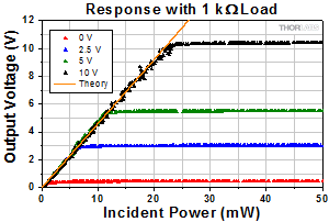

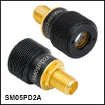
 Zoom
Zoom
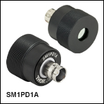


 Mounted Photodiodes