 Products Home
Free-Space InAsSb Amplified Detector
- Broadband Wavelength Sensitivity: 2.7 - 5.3 µm
- Monitor CW or Fast Pulsed Lasers
- Fixed Transimpedance Gain
- Integrate with Cage or Lens Tube Systems
PDA07P2
Fixed Gain
9 MHz Small Signal Bandwidth
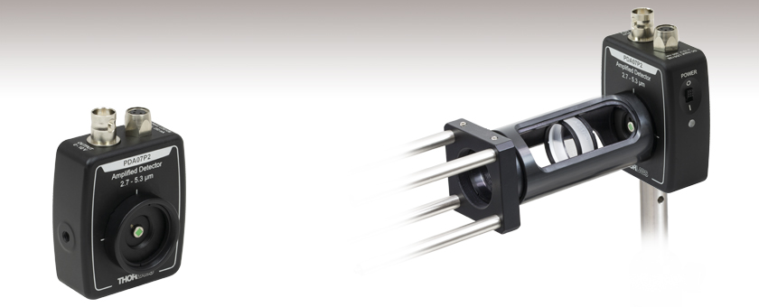
Application Idea
PDA07P2 with Ø1" Lens Tube Attached to a 30 mm Cage System


Please Wait
| MIR Detector Selection Guidea | ||||
|---|---|---|---|---|
| Item # (Detector) | Detector Type | Wavelength Range |
Maximum Bandwidth |
Thermoelectric Cooler |
| PDA10DT (InGaAs) | Photodiode | 0.9 - 2.57 µm | 1,000 kHz | Yes |
| PDA10D2 (InGaAs) | Photodiode | 0.9 - 2.6 µm | 25,000 kHz | No |
| PDA10PT (InAsSb) | Photodiode | 1.0 - 5.8 µm | 1,600 kHz | Yes |
| PDA07P2 (InAsSb) | Photodiode | 2.7 - 5.3 µm | 9 MHz | No |
| PDAVJ8 (HgCdTe) | Photodiode | 2.0 - 8.0 µm | 100 MHz | No |
| PDAVJ10 (HgCdTe) | Photodiode | 2.0 - 10.6 µm | 100 MHz | No |
| PDAVJ5 (HgCdTe) | Photodiode | 2.7 - 5.0 µm | 1 MHz | No |
| PDA13L2 (LiTaO3) | Pyroelectric | 0.6 - 16 µm | 10 kHz | No |

Click to Enlarge
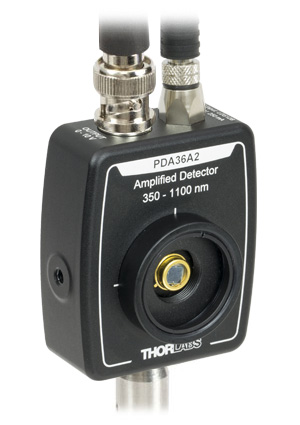
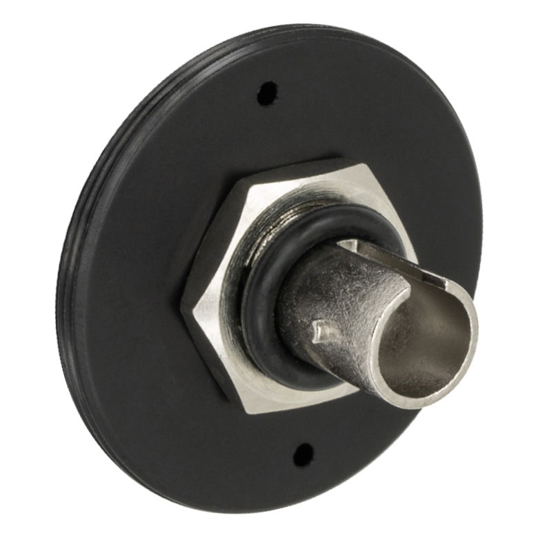
The PDA07P2 has internal SM05 and external SM1 threads and includes an
SM1T1 Internal SM1 Adapter
and SM1RR Retaining Ring.

Click to Enlarge
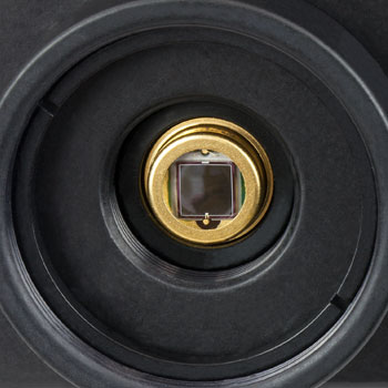
The back plate of the PDA07P2 is engraved with the detector's responsivity curve at 25 °C ambient temperature.
Features
- Wavelength Range from 2.7 to 5.3 µm
- Low-Noise, Wideband Transimpedance Amplifier
- 4.5 mA/W Typical Peak Response
- 9 MHz Small Signal Bandwidth (DC Coupled)
- Post Mountable in Two Orientations Using Universal 8-32 / M4 Taps
- External SM1 (1.035"-40) and Internal SM05 (0.535"-40) Threading
- Linear Power Supply and Location-Specific Power Adapter Included
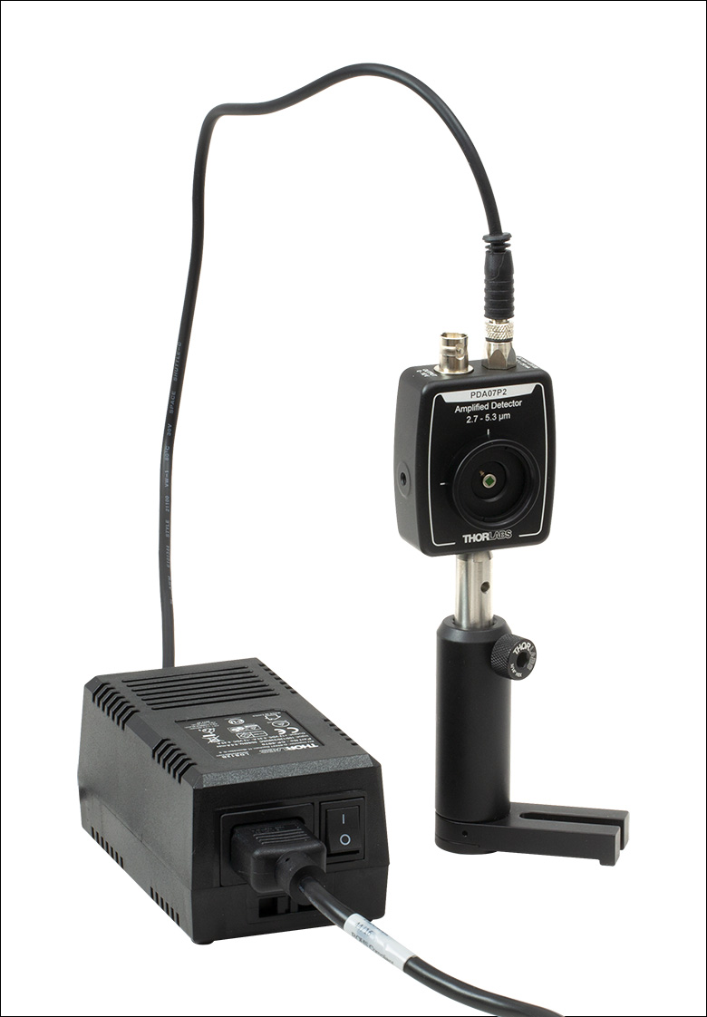
The PDA07P2 is an InAsSb (indium arsenide antimonide)-based, transimpedance-amplified photodetector that is sensitive to light in the MIR spectral range, specifically from 2.7 µm to 5.3 µm. This fixed-gain detector features a 3 x 10⁵ V/A high-impedance gain and is housed in a compact, low-profile package that is ideal for use in light paths with space constraints. The maximum output of the PDA07P2 is
10 V for high-impedance loads (i.e., RLoad > 5 kΩ) and 5 V for 50 Ω loads. Signal output is via a DC-coupled BNC connector. Thorlabs offers numerous BNC, BNC-to-SMA, and SMC cables as well as a variety of BNC, SMA, and SMC adapters.
Since this detector features a 50 Ω load at the output of the BNC connector, it can be used with Thorlabs' passive high-pass filters, which have a low-impedance input of 50 Ω and a high-impedance output that allows them to be directly attached to high-impedance measurement devices such as an oscilloscope. Thus, only use the high-pass filter and detector with oscilloscopes with a high impedance input. Many high-speed oscilloscopes have input impedances of 50 Ω, so we do not recommend installing a 50 Ω terminator. The combined loads will equal 25 Ω, which could allow ~135 mA of output current, damaging the output driver of the PDA07P2.
Click to Enlarge
PDA07P2 Shown with Included Power Supply
The housing of the PDA07P2 features external SM1 (1.035"-40) threading, internal SM05 (0.535"-40) threading, and two universal mounting holes that accept both 8-32 and M4 threads, allowing for either vertical or horizontal post mounting. Addtionally, an SM1T1 internally threaded SM1 coupler and SM1RR retaining ring are included, allowing convenient mounting of SM1-compatible accessories, optics, and cage assembly accessories. The SM1 (1.035"-40) threading on the housing is ideally suited for mounting a Ø1" focusing lens or pinhole in front of the detector element. The internal SM05 threading is only suitable for mating to an externally threaded SM05 lens tube (components such as fiber adapters cannot be threaded onto the SM05 threading). Most SM1-threaded fiber adapters are compatible with this detector. However, the S120-FC, S120- FC2, and S120-25 internally SM1-threaded fiber adapters are not compatible because they collide with the photodiode. Externally SM1-threaded adapters should be mated to the included internally SM1-threaded adapter, while internally SM1-threaded adapters can be mated directly to the housing. See below for our selection of SM1 thread adapters.
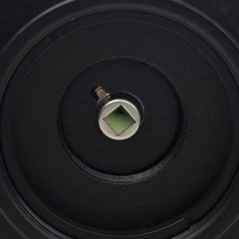
The active area of the photodetector is flush with the front of the housing, simplifying alignments within optomechanical systems. Inhomogeneities at the edges of the active area of the photodetector can generate unwanted capacitance and resistance effects that distort the time-domain response of the photodetector output. Therefore, Thorlabs recommends centering the incident light onto the photodetector's active area. For a detailed drawing of the detector, please see the diagram under the Housing Features column below. We do not recommend exceeding a power density of 1 W/cm2 for light incident on the detector's active area.
Power Supply
A ±12 V linear power supply is included with the amplified photodetector and also available separately below. The power supply features a three-way switch and can be plugged into any 50 to 60 Hz, 100 V / 120 V / 230 V power outlet. Before connecting the power supply to an outlet or to the detector, make sure that the power switches on both the power supply and the detector are in the off position. Hot-plugging is not recommended.
InAsSb Detector with TEC
Thorlabs offers a thermoelectrically cooled InAsSb photodetector (item # PDA10PT). This detector features a thermoelectric cooler (TEC), which uses a thermistor feedback loop to hold the temperature of the detector element at -30 °C, minimizing thermal contributions to the output signal. InAsSb material is naturally temperature dependent, which means the responsivity will be a function of the temperature. Thus, for applications involving changes in ambient temperature, we recommend using the PDA10PT instead of the PDA07P2. For more information about the PDA10PT, please click here.
Click to Enlarge
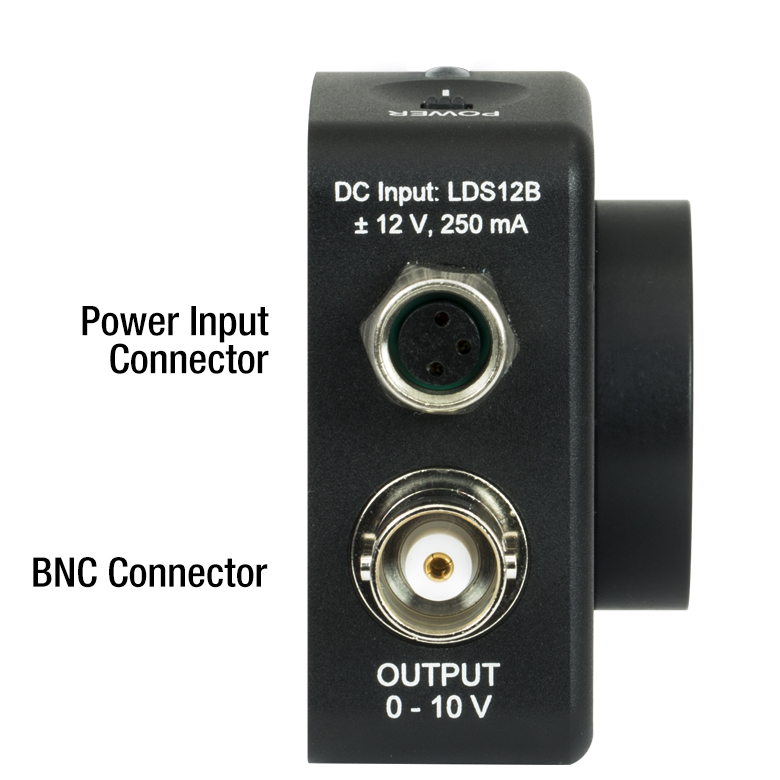
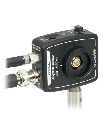
The power input and DC-coupled BNC connector are located at the top of the housing.
Click to Enlarge
The detector has internal SM05 and external SM1 threads and includes an
SM1T1 Internal SM1 Adapter
and SM1RR Retaining Ring.
PDA Series Housing Features
Thorlabs' PDA07P2 is a compact InAsSb amplified photodetector with a fixed gain. This detector's housing features internal SM05 (0.535"-40) threading and external SM1 (1.035"-40) threading. It includes an SM1T1 internally SM1-threaded adapter and SM1RR retaining ring. Most SM1-threaded fiber adapters are compatible with this detector.
Threaded holes on the housing allow the unit to be mounted in a horizontal or vertical orientation, which gives the user the option to route the power and BNC cables from above or alongside the beam path. The PDA07P2 housing features the active area flush with the front of the housing, simplifying alignments within optomechanical systems. This design also has two universal-threaded holes compatible with both 8-32 and M4 threads (see the table below). As a convenience, the back panel is engraved with the responsivity curve of the photodiode. For more information on mounting these units, please see the Mounting Options tab.
| Housing Drawing (Click Icon for Details) |
Mounting Taps | SM Thread Compatibility | Dimensions | Output Connector |
|---|---|---|---|---|
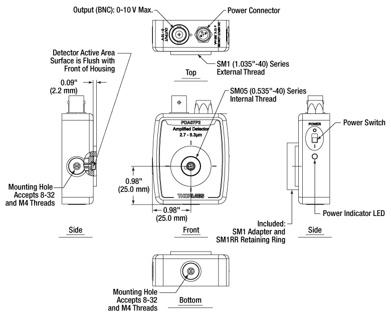 |
Two Universal Taps for 8-32 and M4 |
Internal SM05 (0.535"-40) External SM1 (1.035"-40) |
1.96" x 0.89" x 2.79" (49.8 mm x 22.5 mm x 70.9 mm) |
BNC (DC Coupled) |
PDA and PDF Series Mounting Options
The PDA series of amplified photodetectors are compatible with our entire line of lens tubes, TR series posts, and cage mounting systems. Because of the wide range of mounting options, the best method for mounting the housing in a given optical setup is not always obvious. The pictures and text in this tab will discuss some of the common mounting solutions. As always, our technical support staff is available for individual consultation.
 |
 |
 |
| Picture of a PDA series photodetector as it will look when unpackaged. | Picture of a PDA series photodetector with the included SM1T1 and its retaining ring removed from the front of the housing. Thorlabs' DET series photodetectors feature the same mounting options. | A close up picture of the front of the PDA36A2 photodetector. The internal SM1 threading on the SM1T1 adapter and internal SM05 threading on the photodetector housing can be seen in this image. |
TR Series Post (Ø1/2" Posts) System
The PDA housing can be mounted vertically or horizontally on a TR Series Post using the threaded holes for 8-32 (M4 on metric versions). Select PDA housings feature universally threaded holes for both 8-32 and M4 threads.
 |
 |
| PDA series photodetector mounted vertically on a TR series post. In this configuration, the output and power cables (PDA series) are oriented vertically and away from the optic table, facilitating a neater optical setup. | PDA series photodetector mounted horizontally on a TR series post. In this configuration, the on/off switch is conveniently oriented on the top of the detector. |
Lens Tube System
Each PDA housing includes a detachable Ø1" Optic Mount (SM1T1) that allows for Ø1" (Ø25.4 mm) optical components, such as optical filters and lenses, to be mounted along the axis perpendicular to the center of the photosensitive region. The maximum thickness of an optic that can be mounted in the SM1T1 is 0.1" (2.8 mm). For thicker Ø1" (Ø25.4 mm) optics or for any thickness of Ø0.5" (Ø12.7 mm) optics, remove the SM1T1 from the front of the detector and place (must be purchased separately) an SM1 or SM05 series lens tube, respectively, on the front of the detector.
The SM1 and SM05 threadings on the PDA photodetector housing make it compatible with our SM lens tube system and accessories. Two particularly useful accessories include the SM-threaded irises and the SM-compatible IR and visible alignment tools. Also available are fiber optic adapters for use with connectorized fibers.
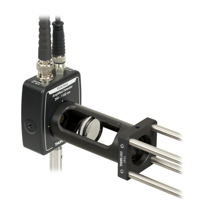 |
| PDA series photodetector mounted onto a Ø1" Slotted Lens Tube, which is housing a focusing optic. The lens tube is attached to a 30 mm cage system via a CP33 SM1-Threaded 30 mm Cage Plate. This arrangement allows easy access for optic adjustment and signal alignment. |
Cage System
The simplest method for attaching the PDA photodetector housing to a cage plate is to remove the SM1T1 that is attached to the front of the PDA and use the external SM1 threads. A cage plate, such as the CP33 30 mm cage plate, can be directly attached to the SM1 threads. Then the retaining ring, included with the SM1T1, can be threaded using a spanner wrench into the CP33 to ensure the cage plate is tightened to the desired location and square with the photodetector housing.
This method for attaching the PDA photodetector housing to a cage plate does not allow much freedom in determining the orientation of the photodetector; however, it has the benefit of not needing an adapter piece, and it allows the diode to be as close as possible to the cage plate, which can be important in setups where the light is divergent. As a side note, Thorlabs sells the SM05PD and SM1PD series of photodiodes that can be threaded into a cage plate so that the diode is flush with the front surface of the cage plate; however, the photodiode is unbiased.
For more freedom in choosing the orientation of the PDA photodetector housing when attaching it, an SM1T2 lens tube coupler can be purchased. In this configuration the SM1T1 is left on the detector and the SM1T2 is threaded into it. The exposed external SM1 threading is now deep enough to secure the detector to a CP33 cage plate in any orientation and lock it into place using one of the two locking rings on the SM1T2.
 |
|
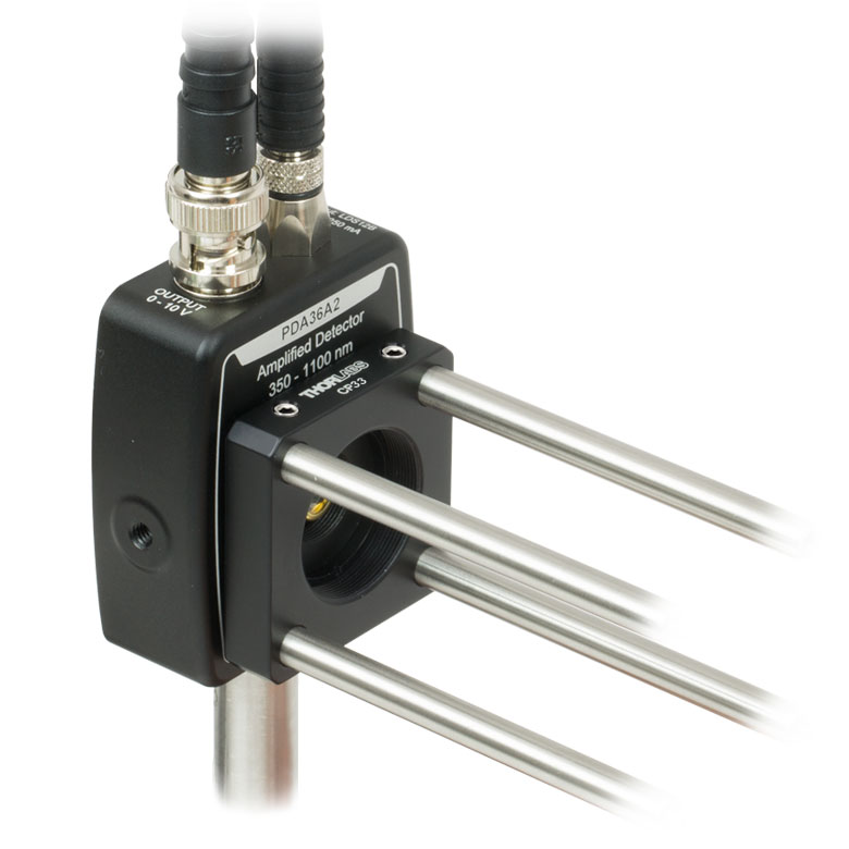
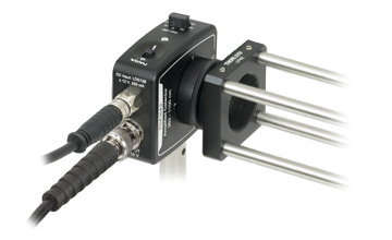
| This picture shows a PDA series photodetector attached to a CP33 cage plate after removing the SM1T1. The retaining ring from the SM1T1 was used to make the orientation of the detector square with the cage plate. | These two pictures show a PDA series photodetector in a horizontal configuration. The top picture shows the detector directely coupled to a CP33 cage plate. The bottom picture shows a PDA series photodetector attached to a CP33 cage plate using an SM1T2 adapter in addition to the SM1T1 that comes with the PDA series detector. |

Although not pictured here, the PDA photodetector housing can be connected to a 16 mm cage system by purchasing an SM05T2. It can be used to connect the PDA photodetector housing to an SP02 cage plate.
Application
The image below shows a Michelson Interferometer built entirely from parts available from Thorlabs. This application demonstrates the ease with which an optical system can be constructed using our lens tube, TR series post, and cage systems.
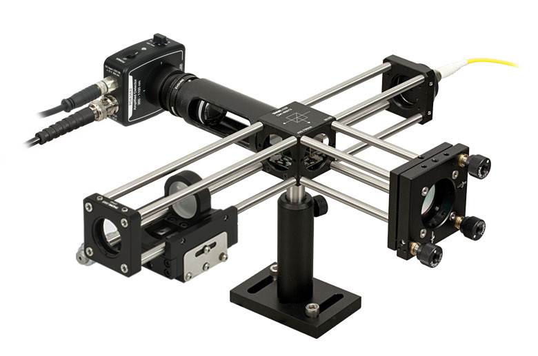 |
The table below contains a part list for the Michelson Interferometer for use in the visible range. Follow the links to the pages for more information about the individual parts.
| Item # | Quantity | Description | Item # | Quantity | Description |
|---|---|---|---|---|---|
| KC1 | 1 | Mirror Mount | CT1A | 1 | 1/2" Travel Translator |
| BB1-E02 | 2 | Broadband Dielectric Laser Mirrors | SM1D12 | 1 | SM1 Threaded Lens Tube Iris |
| ER4 | 8 | 4" Cage Rods | SM1L30C | 1 | SM1 3" Slotted Lens Tube |
| ER6 | 4 | 6" Cage Rods | SM1V05 | 1 | Ø1" Adjustable Length Lens Tube |
| CCM1-BS013 | 1 | Cube-Mounted Beamsplitter | CP08FP | 1 | 30 mm Cage Plate for FiberPorts |
| BA2 | 1 | Post Base (not shown in picture) | PAF2-5A | 1 | FiberPort |
| TR2 | 1 | Ø1/2" Post, 2" in Length | P1-460B-FC-2 | 1 | Single Mode Fiber Patch Cable |
| PH2 | 1 | Ø1/2" Post Holder | DET36A / PDA36A2 | 1 | Biased / Amplified Photodiode Detector |
BNC Female Output, DC Coupled
(Photodetector)
0 - 5 V at 50 Ω
0 - 10 V at Hi-Z
100 mA Max Current
PDA Male (Power Cables)
PDA Female (Photodetector)
Photodiode Tutorial
Theory of Operation
A junction photodiode is an intrinsic device that behaves similarly to an ordinary signal diode, but it generates a photocurrent when light is absorbed in the depleted region of the junction semiconductor. A photodiode is a fast, highly linear device that exhibits high quantum efficiency and may be used in a variety of different applications.
It is necessary to be able to correctly determine the level of the output current to expect and the responsivity based upon the incident light. Depicted in Figure 1 is a junction photodiode model with basic discrete components to help visualize the main characteristics and gain a better understanding of the operation of Thorlabs' photodiodes.
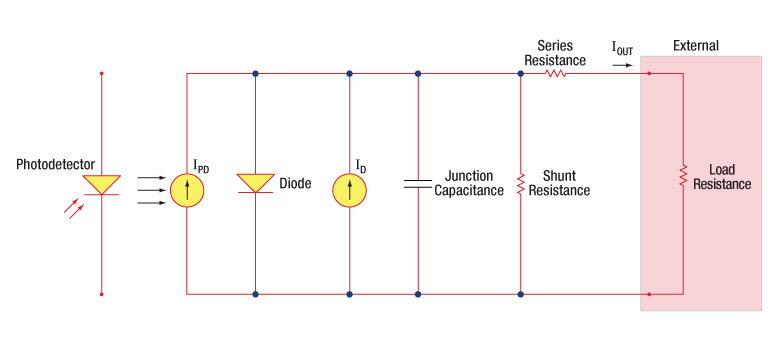
Figure 1: Photodiode Model
Photodiode Terminology
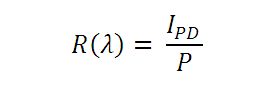
Responsivity
The responsivity of a photodiode can be defined as a ratio of generated photocurrent (IPD) to the incident light power (P) at a given wavelength:
Modes of Operation (Photoconductive vs. Photovoltaic)
A photodiode can be operated in one of two modes: photoconductive (reverse bias) or photovoltaic (zero-bias). Mode selection depends upon the application's speed requirements and the amount of tolerable dark current (leakage current).
Photoconductive
In photoconductive mode, an external reverse bias is applied, which is the basis for our DET series detectors. The current measured through the circuit indicates illumination of the device; the measured output current is linearly proportional to the input optical power. Applying a reverse bias increases the width of the depletion junction producing an increased responsivity with a decrease in junction capacitance and produces a very linear response. Operating under these conditions does tend to produce a larger dark current, but this can be limited based upon the photodiode material. (Note: Our DET detectors are reverse biased and cannot be operated under a forward bias.)
Photovoltaic
In photovoltaic mode the photodiode is zero biased. The flow of current out of the device is restricted and a voltage builds up. This mode of operation exploits the photovoltaic effect, which is the basis for solar cells. The amount of dark current is kept at a minimum when operating in photovoltaic mode.
Dark Current
Dark current is leakage current that flows when a bias voltage is applied to a photodiode. When operating in a photoconductive mode, there tends to be a higher dark current that varies directly with temperature. Dark current approximately doubles for every 10 °C increase in temperature, and shunt resistance tends to double for every 6 °C rise. Of course, applying a higher bias will decrease the junction capacitance but will increase the amount of dark current present.
The dark current present is also affected by the photodiode material and the size of the active area. Silicon devices generally produce low dark current compared to germanium devices which have high dark currents. The table below lists several photodiode materials and their relative dark currents, speeds, sensitivity, and costs.
| Material | Dark Current | Speed | Spectral Range | Cost |
|---|---|---|---|---|
| Silicon (Si) | Low | High Speed | Visible to NIR | Low |
| Germanium (Ge) | High | Low Speed | NIR | Low |
| Gallium Phosphide (GaP) | Low | High Speed | UV to Visible | Moderate |
| Indium Gallium Arsenide (InGaAs) | Low | High Speed | NIR | Moderate |
| Indium Arsenide Antimonide (InAsSb) | High | Low Speed | NIR to MIR | High |
| Extended Range Indium Gallium Arsenide (InGaAs) | High | High Speed | NIR | High |
| Mercury Cadmium Telluride (MCT, HgCdTe) | High | Low Speed | NIR to MIR | High |
Junction Capacitance
Junction capacitance (Cj) is an important property of a photodiode as this can have a profound impact on the photodiode's bandwidth and response. It should be noted that larger diode areas encompass a greater junction volume with increased charge capacity. In a reverse bias application, the depletion width of the junction is increased, thus effectively reducing the junction capacitance and increasing the response speed.
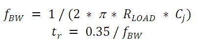
Bandwidth and Response
A load resistor will react with the photodetector junction capacitance to limit the bandwidth. For best frequency response, a 50 Ω terminator should be used in conjunction with a 50 Ω coaxial cable. The bandwidth (fBW) and the rise time response (tr) can be approximated using the junction capacitance (Cj) and the load resistance (RLOAD):
Noise Equivalent Power
The noise equivalent power (NEP) is the generated RMS signal voltage generated when the signal to noise ratio is equal to one. This is useful, as the NEP determines the ability of the detector to detect low level light. In general, the NEP increases with the active area of the detector and is given by the following equation:

Here, S/N is the Signal to Noise Ratio, Δf is the Noise Bandwidth, and Incident Energy has units of W/cm2. For more information on NEP, please see Thorlabs' Noise Equivalent Power White Paper.
Terminating Resistance
A load resistance is used to convert the generated photocurrent into a voltage (VOUT) for viewing on an oscilloscope:
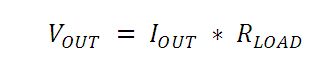
Depending on the type of the photodiode, load resistance can affect the response speed. For maximum bandwidth, we recommend using a 50 Ω coaxial cable with a 50 Ω terminating resistor at the opposite end of the cable. This will minimize ringing by matching the cable with its characteristic impedance. If bandwidth is not important, you may increase the amount of voltage for a given light level by increasing RLOAD. In an unmatched termination, the length of the coaxial cable can have a profound impact on the response, so it is recommended to keep the cable as short as possible.
Shunt Resistance
Shunt resistance represents the resistance of the zero-biased photodiode junction. An ideal photodiode will have an infinite shunt resistance, but actual values may range from the order of ten Ω to thousands of MΩ and is dependent on the photodiode material. For example, and InGaAs detector has a shunt resistance on the order of 10 MΩ while a Ge detector is in the kΩ range. This can significantly impact the noise current on the photodiode. For most applications, however, the high resistance produces little effect and can be ignored.
Series Resistance
Series resistance is the resistance of the semiconductor material, and this low resistance can generally be ignored. The series resistance arises from the contacts and the wire bonds of the photodiode and is used to mainly determine the linearity of the photodiode under zero bias conditions.
Common Operating Circuits
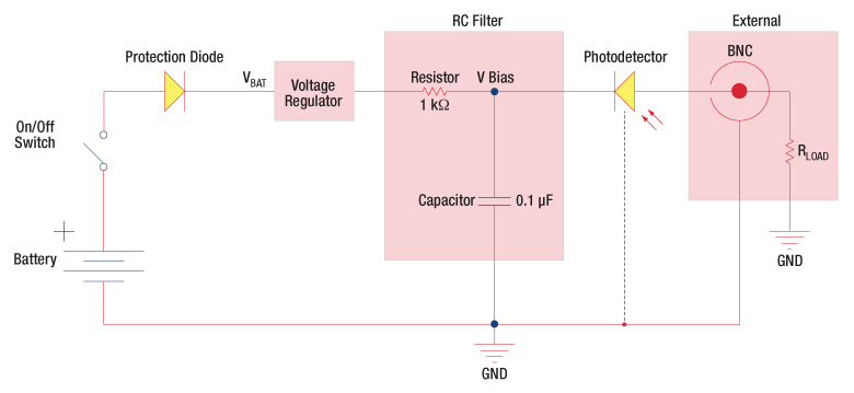
Figure 2: Reverse-Biased Circuit (DET Series Detectors)
The DET series detectors are modeled with the circuit depicted above. The detector is reverse biased to produce a linear response to the applied input light. The amount of photocurrent generated is based upon the incident light and wavelength and can be viewed on an oscilloscope by attaching a load resistance on the output. The function of the RC filter is to filter any high-frequency noise from the input supply that may contribute to a noisy output.
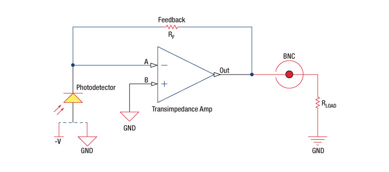
Figure 3: Amplified Detector Circuit
One can also use a photodetector with an amplifier for the purpose of achieving high gain. The user can choose whether to operate in Photovoltaic of Photoconductive modes. There are a few benefits of choosing this active circuit:
- Photovoltaic mode: The circuit is held at zero volts across the photodiode, since point A is held at the same potential as point B by the operational amplifier. This eliminates the possibility of dark current.
- Photoconductive mode: The photodiode is reversed biased, thus improving the bandwidth while lowering the junction capacitance. The gain of the detector is dependent on the feedback element (Rf). The bandwidth of the detector can be calculated using the following:
where GBP is the amplifier gain bandwidth product and CD is the sum of the junction capacitance and amplifier capacitance.
Effects of Chopping Frequency
The photoconductor signal will remain constant up to the time constant response limit. Many detectors, including PbS, PbSe, HgCdTe (MCT), and InAsSb, have a typical 1/f noise spectrum (i.e., the noise decreases as chopping frequency increases), which has a profound impact on the time constant at lower frequencies.
The detector will exhibit lower responsivity at lower chopping frequencies. Frequency response and detectivity are maximized for
![]()
Pulsed Laser Emission: Power and Energy Calculations

Determining whether emission from a pulsed laser is compatible with a device or application can require referencing parameters that are not supplied by the laser's manufacturer. When this is the case, the necessary parameters can typically be calculated from the available information. Calculating peak pulse power, average power, pulse energy, and related parameters can be necessary to achieve desired outcomes including:
- Protecting biological samples from harm.
- Measuring the pulsed laser emission without damaging photodetectors and other sensors.
- Exciting fluorescence and non-linear effects in materials.
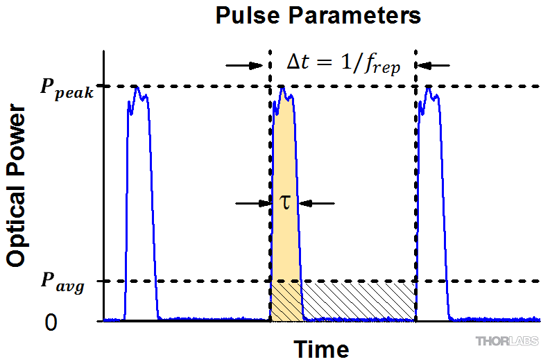
Pulsed laser radiation parameters are illustrated in Figure 1 and described in the table. For quick reference, a list of equations are provided below. The document available for download provides this information, as well as an introduction to pulsed laser emission, an overview of relationships among the different parameters, and guidance for applying the calculations.
|
Equations: |
||||
 |
and |  |
||
 |
||||
 |
||||
 |
||||
Peak power and average power calculated from each other: |
||||
 |
and |  |
||
| Peak power calculated from average power and duty cycle*: | ||||
 |
*Duty cycle ( ) is the fraction of time during which there is laser pulse emission. ) is the fraction of time during which there is laser pulse emission. |
|||
Click to Enlarge
Figure 1: Parameters used to describe pulsed laser emission are indicated in the plot (above) and described in the table (below). Pulse energy (E) is the shaded area under the pulse curve. Pulse energy is, equivalently, the area of the diagonally hashed region.
| Parameter | Symbol | Units | Description | ||
|---|---|---|---|---|---|
| Pulse Energy | E | Joules [J] | A measure of one pulse's total emission, which is the only light emitted by the laser over the entire period. The pulse energy equals the shaded area, which is equivalent to the area covered by diagonal hash marks. | ||
| Period | Δt | Seconds [s] | The amount of time between the start of one pulse and the start of the next. | ||
| Average Power | Pavg | Watts [W] | The height on the optical power axis, if the energy emitted by the pulse were uniformly spread over the entire period. | ||
| Instantaneous Power | P | Watts [W] | The optical power at a single, specific point in time. | ||
| Peak Power | Ppeak | Watts [W] | The maximum instantaneous optical power output by the laser. | ||
| Pulse Width |  |
Seconds [s] | A measure of the time between the beginning and end of the pulse, typically based on the full width half maximum (FWHM) of the pulse shape. Also called pulse duration. | ||
| Repetition Rate | frep | Hertz [Hz] | The frequency with which pulses are emitted. Equal to the reciprocal of the period. | ||
Example Calculation:
Is it safe to use a detector with a specified maximum peak optical input power of 75 mW to measure the following pulsed laser emission?
- Average Power: 1 mW
- Repetition Rate: 85 MHz
- Pulse Width: 10 fs
The energy per pulse:

seems low, but the peak pulse power is:

It is not safe to use the detector to measure this pulsed laser emission, since the peak power of the pulses is >5 orders of magnitude higher than the detector's maximum peak optical input power.
The following table lists Thorlabs' selection of photodiodes, photoconductive, and pyroelectric detectors. Item numbers in the same row contain the same detector element.
| Photodetector Cross Reference | ||||||
|---|---|---|---|---|---|---|
| Wavelength | Material | Unmounted Photodiode |
Mounted Photodiode |
Biased Detector |
Amplified Detector |
Amplified Detector, OEM Package |
| 200 - 1100 nm | Si | FDS010 | SM05PD2A SM05PD2B |
DET10A2 | PDA10A2 | - |
| Si | - | SM1PD2A | - | - | - | |
| 240 - 1170 nm | B-Si | - | - | DET20X2 | - | - |
| 320 - 1000 nm | Si | - | - | - | PDA8A2 | - |
| 320 - 1100 nm | Si | FD11A | SM05PD3A | - | PDF10A2 | - |
| Si | - a | - | DET100A2 a | PDA100A2 a | PDAPC2 a | |
| 340 - 1100 nm | Si | FDS10X10 | - | - | - | - |
| 350 - 1100 nm | Si | FDS100 FDS100-CAL b |
SM05PD1A SM05PD1B |
DET36A2 | PDA36A2 | PDAPC1 |
| Si | FDS1010 FDS1010-CAL b |
SM1PD1A SM1PD1B |
- | - | - | |
| 400 - 1000 nm | Si | - | - | - | PDA015A2 FPD310-FS-VIS FPD310-FC-VIS FPD510-FC-VIS FPD510-FS-VIS FPD610-FC-VIS FPD610-FS-VIS |
- |
| 400 - 1100 nm | Si | FDS015 c | - | - | - | - |
| Si | FDS025 c FDS02 d |
- | DET02AFC(/M) DET025AFC(/M) DET025A(/M) DET025AL(/M) |
- | - | |
| 400 - 1700 nm | Si & InGaAs | DSD2 | - | - | - | - |
| 500 - 1700 nm | InGaAs | - | - | DET10N2 | - | - |
| 0.6 - 16 µm | LiTaO3 | - | - | - | PDA13L2e | - |
| 750 - 1650 nm | InGaAs | - | - | - | PDA8GS | - |
| 800 - 1700 nm | InGaAs | FGA015 | - | - | PDA015C2 | - |
| InGaAs | FGA21 FGA21-CAL b |
SM05PD5A | DET20C2 | PDA20C2 PDA20CS2 |
- | |
| InGaAs | FGA01 c FGA01FC d |
- | DET01CFC(/M) | - | - | |
| InGaAs | FDGA05 c | - | - | PDA05CF2 | - | |
| InGaAs | - | - | DET08CFC(/M) DET08C(/M) DET08CL(/M) |
- | - | |
| InGaAs | - | - | - | PDF10C2 | - | |
| 800 - 1800 nm | Ge | FDG03 FDG03-CAL b |
SM05PD6A | DET30B2 | PDA30B2 | - |
| Ge | FDG50 | - | DET50B2 | PDA50B2 | - | |
| Ge | FDG05 | - | - | - | - | |
| 900 - 1700 nm | InGaAs | FGA10 | SM05PD4A | DET10C2 | PDA10CS2 | - |
| 900 - 2600 nm | InGaAs | FD05D | - | DET05D2 | - | - |
| FD10D | - | DET10D2 | PDA10D2 | - | ||
| 950 - 1650 nm | InGaAs | - | - | - | FPD310-FC-NIR FPD310-FS-NIR FPD510-FC-NIR FPD510-FS-NIR FPD610-FC-NIR FPD610-FS-NIR |
- |
| 1.0 - 5.8 µm | InAsSb | - | - | - | PDA10PT(-EC) | - |
| 2.0 - 8.0 µm | HgCdTe (MCT) | VML8T0 VML8T4 f |
- | - | PDAVJ8 | - |
| 2.0 - 10.6 µm | HgCdTe (MCT) | VML10T0 VML10T4 f |
- | - | PDAVJ10 | - |
| 2.7 - 5.0 µm | HgCdTe (MCT) | VL5T0 | - | - | PDAVJ5 | - |
| 2.7 - 5.3 µm | InAsSb | - | - | - | PDA07P2 | - |
| Posted Comments: | |
Michael Kellett
(posted 2024-04-10 08:42:57.473) Hello, we want to make our own power lead for the PDA07P2, can you please tell me the source and part number for a mating power plug for it.
Thanks. Joon hak Park
(posted 2021-12-20 22:33:11.04) I recently have the PDA07P2. I detected the pulse width of a Er:YAG laser. But the pulse shape confused me with being fluctuated. I am not sure whether I use it well or not. Could I ask your about it more? cdolbashian
(posted 2022-01-25 04:43:07.0) Thank you for reaching out to us at Thorlabs. I have reached out to you directly to troubleshoot the problems you are seeing with your particular application. In the future, technical support issues can be sent directly to techsupport@thorlabs.com for the fastest response. Kevin Lehmann
(posted 2021-05-28 14:02:25.637) I just received one of these. I want to know what is the maximum optical power (cw) that the detector can handle. I don't want to damage it! cdolbashian
(posted 2021-06-04 12:03:35.0) Thank you for reaching out to us! All of our photodetectors will saturate electronically before they are optically damaged. Without knowing your wavelength, we cannot predict an input power which will cause this saturation. I have reached out to you directly for more details. 刘贵权 刘
(posted 2020-07-13 13:24:55.703) We want to buy this product YLohia
(posted 2020-07-13 10:35:27.0) Hello, thank you for your interest in our products. Orders can be placed from our website by adding the item to your cart and checking out. Alternately, you may contact your local Thorlabs Sales Team: https://www.thorlabs.com/locations.cfm. |
| Item #a | Housing Featuresb | Active Areac,d | Wavelength Rangee |
Small Signal Bandwidth |
Noise-Equivalent Power (NEP) | Load Impedance |
Transimpedance Gain | Noise (RMS) | Responsivity Data |
Operating Temperature Range |
Power Supply Included |
|---|---|---|---|---|---|---|---|---|---|---|---|
| PDA07P2 | |
0.49 mm2 |
2.7 - 5.3 µm | 9 MHz | 50 Ω to Hi-Z | 1.5 x 10⁵ V/A (50 Ω) 3 x 10⁵ V/A (Hi-Z) |
1 mVrms | 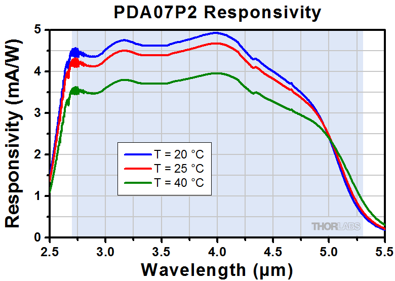 Click Here for Raw Data |
10 to 50 °C | Yes |

 Zoom
Zoom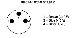
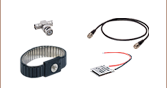
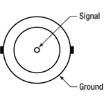
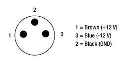
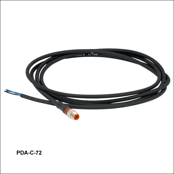
The PDA-C-72 power cord is offered for the PDA line of amplified photodetectors when using with a power supply other than the one included with the detector. The cord has tinned leads on one end and a PDA-compatible 3-pin connector on the other end. It can be used to power the PDA series of amplified photodetectors with any power supply that provides a DC voltage. The pin descriptions are shown to the right.

 Zoom
Zoom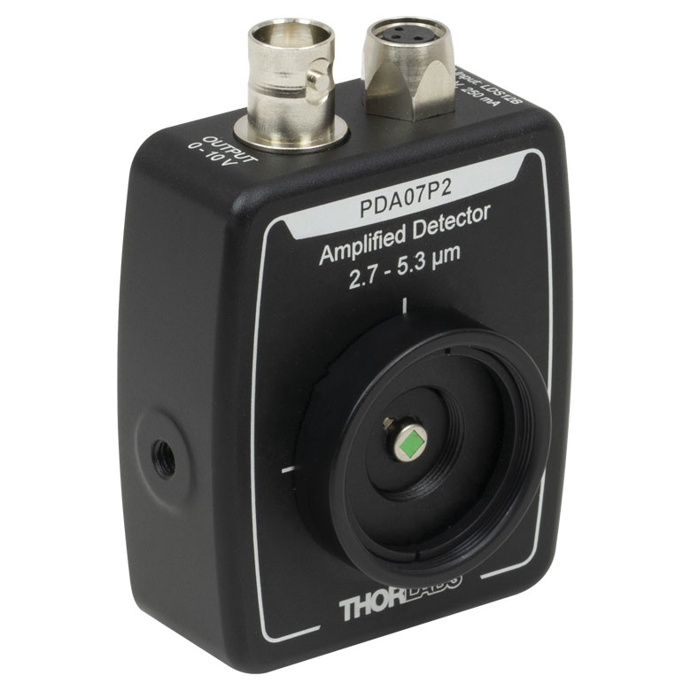
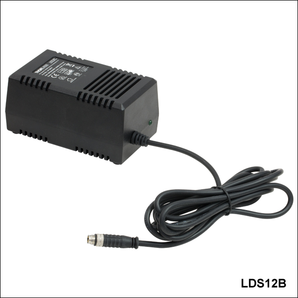
- Replacement Power Supply for the PDA and PDF Amplified Photodetectors Sold Above
- ±12 VDC Power Output
- Current Limit Enabling Short Circuit and Overload Protection
- On/Off Switch with LED Indicator
- Switchable AC Input Voltage (100, 120, or 230 VAC)
- 2 m (6.6 ft) Cable with LUMBERG RSMV3 Male Connector
- UL and CE Compliant
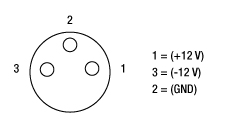
The LDS12B ±12 VDC Regulated Linear Power Supply is intended as a replacement for the supply that comes with our PDA and PDF line of amplified photodetectors sold on this page. The cord has three pins: one for ground, one for +12 V, and one for -12 V (see diagram above). A region-specific power cord is shipped with the LDS12B power supply based on your location. This power supply can also be used with the PDB series of balanced photodetectors, PMM series of photomultiplier modules,APD series of avalanche photodetectors, and the FSAC autocorrelator for femtosecond lasers.
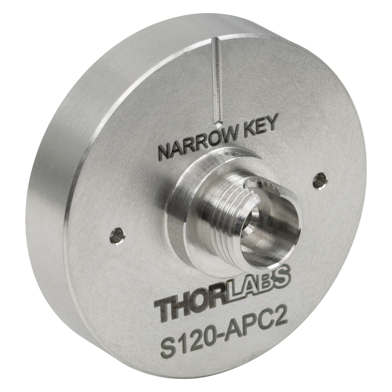
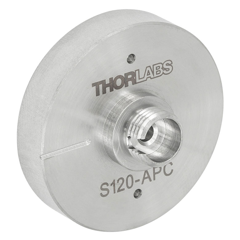
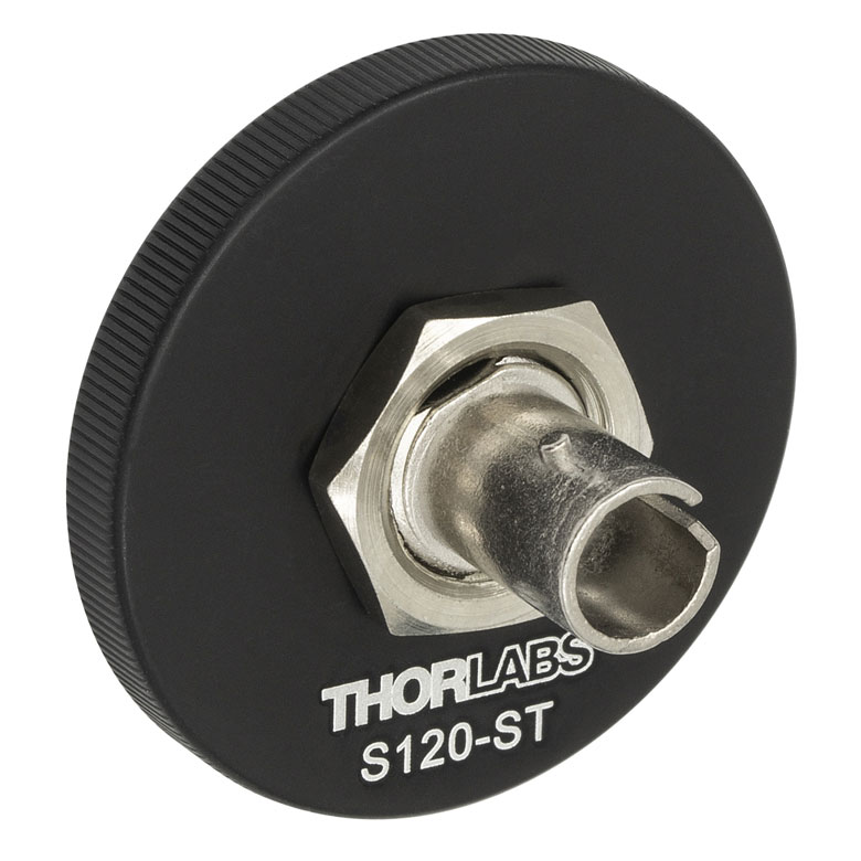
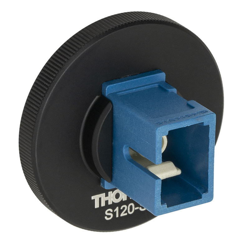
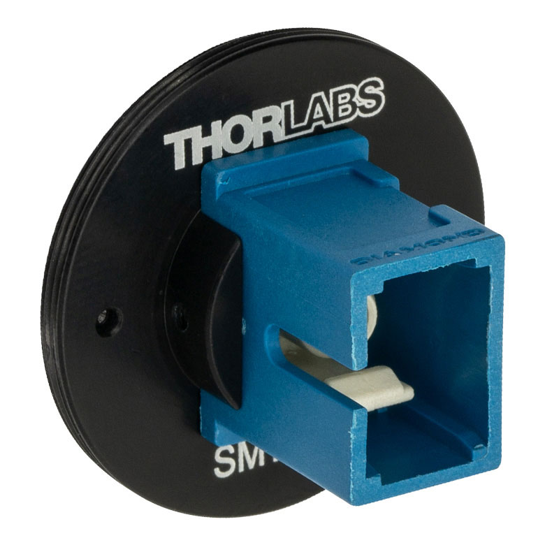
- FC/APC (Narrow Key or Wide Key), SMA, ST®*/PC, SC/PC, or LC/PC Fiber Receptacles.
- Light-Tight Construction When Used with SM1 Lens Tubes
- Compatible with Many of Our Photodiode Power Sensors
Note: The APC adapters have two dimples in the front surface that allow them to be tightened with the SPW909 or SPW801 spanner wrench. The dimples do not go all the way through the disk so that the adapter can be used in light-tight applications when paired with SM1 lens tubes.
FC/APC adapters are available with either narrow (2.0 mm) or wide (2.2 mm) key connectors; for more details on narrow versus wide key connectors, please see our Intro to Fiber tutorial.
| Item # | S120-APC2a | S120-APCa | S120-SMA | S120-ST | S120-SC | S120-LC |
|---|---|---|---|---|---|---|
| Adapter Image (Click the Image to Enlarge) |
 |
 |
 |
 |
 |
 |
| Fiber Connector Type | FC/APC, 2.0 mm Narrow Key |
FC/APC 2.2 mm Wide Key |
SMA | ST/PC | SC/PCb | LC/PC |
| Threading | Internal SM1 (1.035"-40) | |||||
*ST® is a registered trademark of Lucent Technologies, Inc.
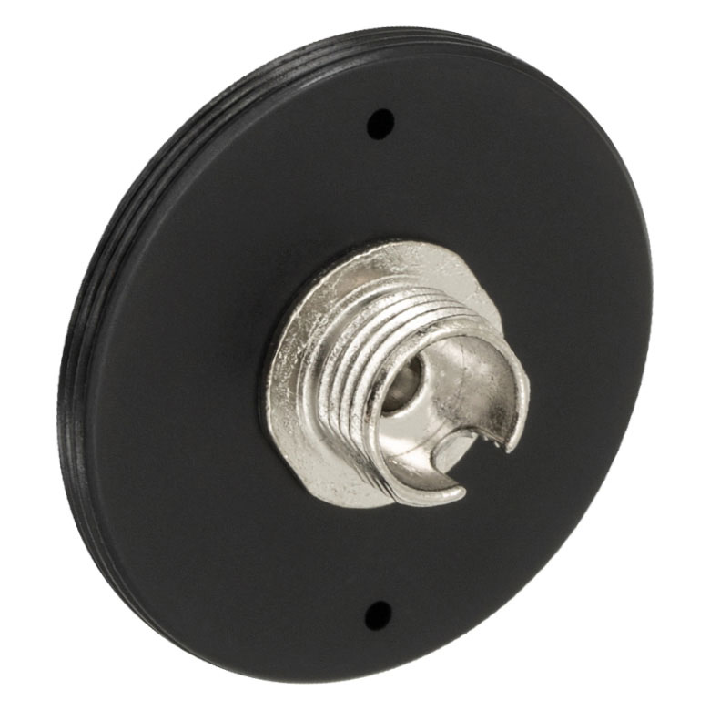
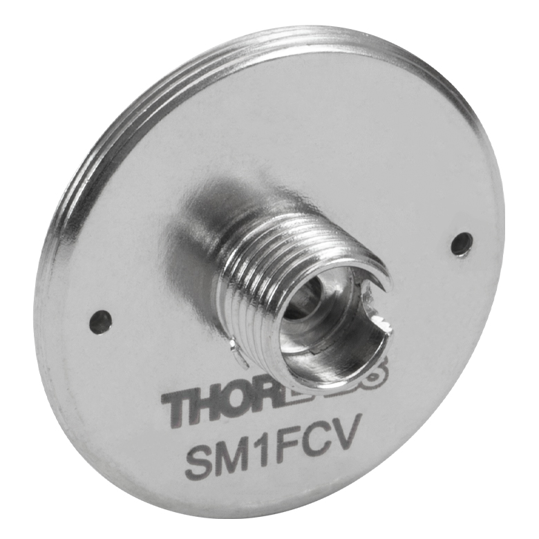
- FC/PC (Narrow or Wide Key), FC/APC (Narrow or Wide Key), SMA, ST®*/PC, SC/PC, or LC/PC Receptacles
- Vacuum-Compatible Versions of FC/PC Wide-Key and SMA Receptacles Available
- Light-Tight When Used with SM1 Lens Tubes
- Compatible with Many of Our 30 mm Cage Plates and Photodetectors
Note: Each disk has four dimples, two in the front surface and two in the back surface, that allow it to be tightened from either side with the SPW909 or SPW801 spanner wrench. The dimples do not go all the way through the disk so that the adapters can be used in light-tight applications when paired with SM1 lens tubes. Once the adapter is at the desired position, use an SM1RR retaining ring to secure it in place.
FC/PC and FC/APC adapters are available with either narrow (2.0 mm) or wide (2.2 mm) key connectors; for more details on narrow versus wide key connectors, please see our Intro to Fiber tutorial.
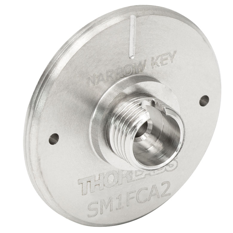
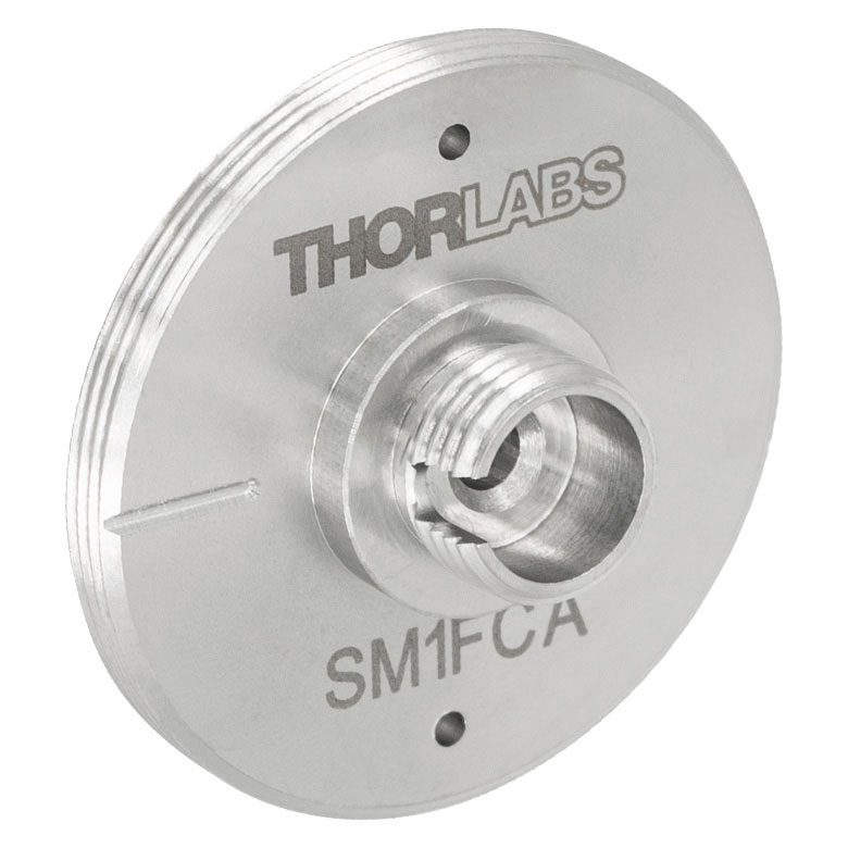
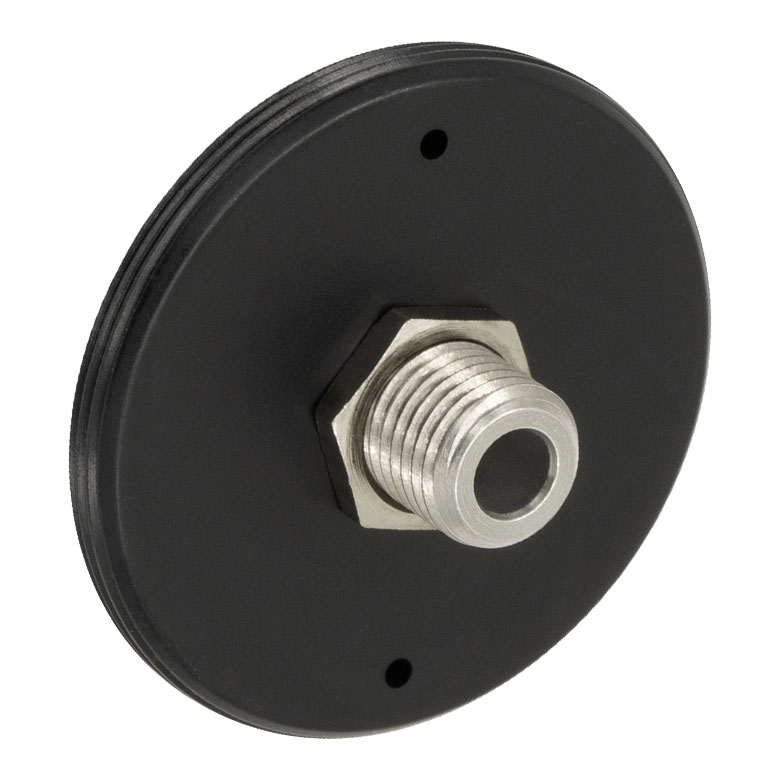
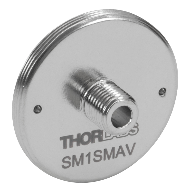
| Item # | SM1FC2 | SM1FC | SM1FCV | SM1FCA2a | SM1FCAa | SM1SMA | SM1SMAV | SM1ST | SM1SC1b | SM1LCb |
|---|---|---|---|---|---|---|---|---|---|---|
| Adapter Image (Click the Image to Enlarge) |
 |
 |
 |
 |
 |
 |
 |
 |
 |
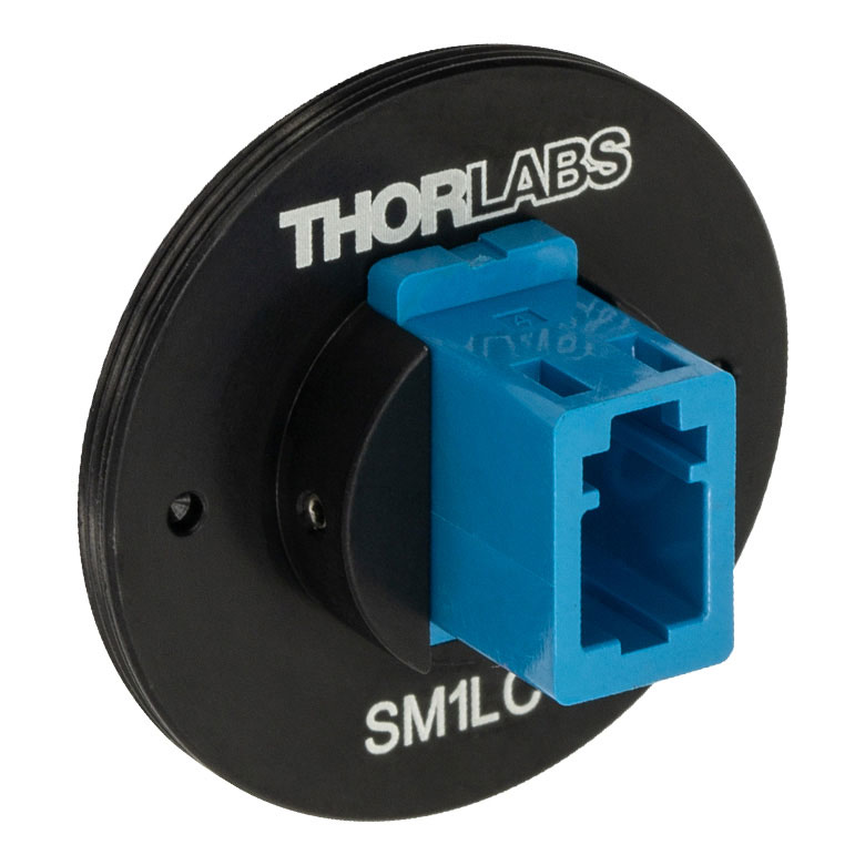 |
| Connector Type | FC/PC, 2.0 mm Narrow Key |
FC/PC, 2.2 mm Wide Key |
FC/PC, 2.2 mm Wide Key |
FC/APC, 2.0 mm Narrow Key |
FC/APC, 2.2 mm Wide Key |
SMA | SMA | ST/PC | SC/PCc | LC/PC |
| Vacuum Compatibility | - | >10-10 Torr | - | >10-10 Torr | - | |||||
| Threading | External SM1 (1.035"-40) | |||||||||
*ST® is a registered trademark of Lucent Technologies, Inc.