 Products Home
Free-Space InAsSb Amplified Detector with TEC
- Broadband Wavelength Sensitivity: 1.0 - 5.8 µm
- Built-In TEC Lowers Thermal Noise
- 8-Step Variable Gain and Bandwidth
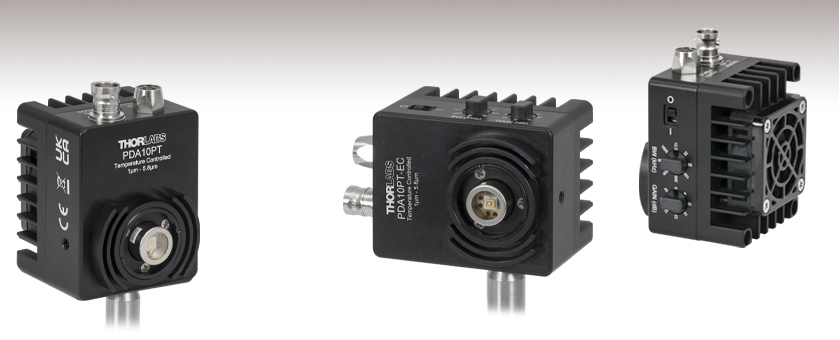
PDA10PT
Post Not Included
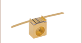
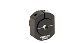
Side Mounted,
Post Not Included
Side View
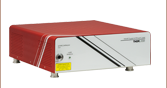
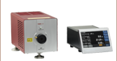
Power Supply
Included with
Detector


Please Wait
| MIR Detector Selection Guidea | ||||
|---|---|---|---|---|
| Item # (Detector) | Detector Type | Wavelength Range |
Maximum Bandwidth |
Thermoelectric Cooler |
| PDA10DT (InGaAs) | Photodiode | 0.9 - 2.57 µm | 1,000 kHz | Yes |
| PDA10D2 (InGaAs) | Photodiode | 0.9 - 2.6 µm | 25,000 kHz | No |
| PDA10PT (InAsSb) | Photodiode | 1.0 - 5.8 µm | 1,600 kHz | Yes |
| PDA07P2 (InAsSb) | Photodiode | 2.7 - 5.3 µm | 9 MHz | No |
| PDAVJ8 (HgCdTe) | Photodiode | 2.0 - 8.0 µm | 100 MHz | No |
| PDAVJ10 (HgCdTe) | Photodiode | 2.0 - 10.6 µm | 100 MHz | No |
| PDAVJ5 (HgCdTe) | Photodiode | 2.7 - 5.0 µm | 1 MHz | No |
| PDA13L2 (LiTaO3) | Pyroelectric | 0.6 - 16 µm | 10 kHz | No |
Features
- Sensitive to Mid-IR (MIR) Light from 1.0 - 5.8 µm
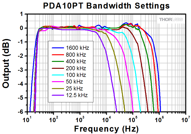
- Max Bandwidth of Detector Package: 1600 kHz
- Built-In Thermoelectric Cooler Improves Sensitivity
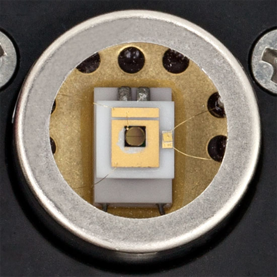
- Ø1 mm Detector Element
- Post Mountable in Two Orientations
- Internally SM1 (1.035"-40) Threaded
- Location-Specific Power Adapter Included
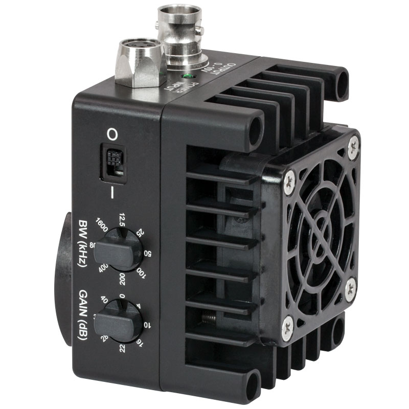
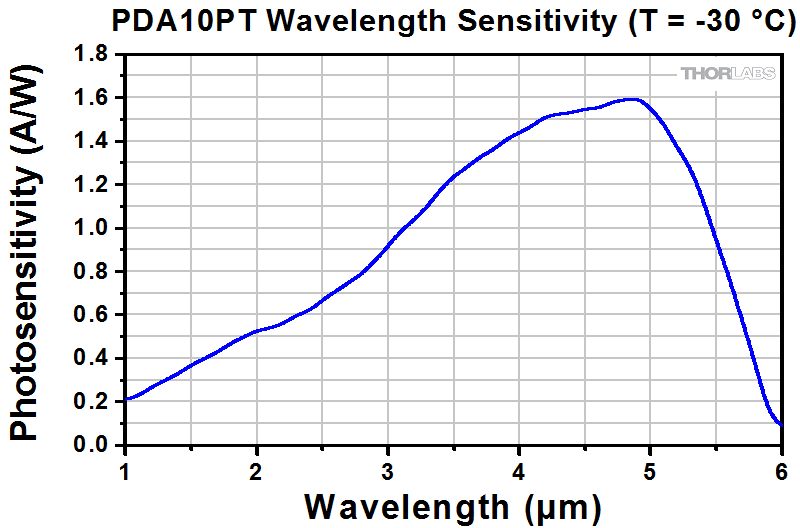
Thorlabs' PDA10PT(-EC) Amplified Detector is a thermoelectrically cooled photoconductive InAsSb (indium arsenide antimonide) detector. Like our HgCdTe (MCT) detector, this material is sensitive to light in the mid-IR spectral range, but the PDA10PT features a broader sensitivity range of 1.0 to 5.8 µm. Two rotary switches control the gain amplifier and detector package bandwidth, allowing performance to be optimized for a variety of applications. The gain switch features eight discrete steps from 0 - 40 dB, while the bandwidth switch provides eight discrete steps from 12.5 kHz - 1600 kHz. The thermoelectric cooler (TEC) uses a thermistor feedback loop to hold the temperature of the detector element at -30 °C, minimizing thermal contributions to the output signal.
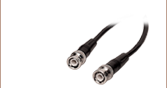
For best results, we recommend connecting the BNC output cable (not included) to a 50 Ω termination. Because the detector is AC coupled, it requires a pulsed or chopped input signal. AC-coupled detectors will not see unchopped CW light because they are only sensitive to intensity changes, not absolute intensity. These photodetectors are ideal for use with Thorlabs' passive low-pass filters; these filters have a 50 Ω input and a high-impedance output that allows them to be directly attached to high-impedance measurement devices such as an oscilloscope.
Click to Enlarge
Side View Showing Gain and Bandwidth Adjusters
Click to Enlarge
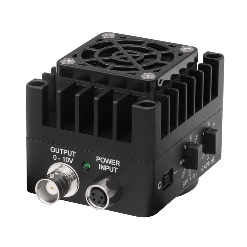
Top View Showing Signal Output and Power Input
The detector package incorporates many of the same mechanical features as our other mounted photodetectors. An internal SM1 (1.035"-40) threading allows Ø1" lens tubes to be mounted in front of the detector element. Two 8-32 (M4 in the -EC version) tapped holes connect a Ø1/2" post to the housing in one of two perpendicular orientations, as shown in the image at the top of the page. The PDA10PT(-EC) includes a 100 - 240 VAC power adapter. If you require a different adapter plug, please contact Tech Support prior to ordering. An SM1RR Retaining Ring is also included.
Please note that inhomogeneities at the edges of the active area of the detector can generate unwanted capacitance and resistance effects that distort the time-domain response of the output. Thorlabs therefore recommends that the incident light is well centered on the active area. The SM1 (1.035"-40) threading on the housing can be connected to an SM1 lens tube; the lens tube can be used to mount an iris or pinhole in front of the detector element. Because the detector package protrudes 3.9 mm beyond the front of the threading, optics and optomechanics cannot be attached directly to the housing.
In addition to the InAsSb detector sold here, Thorlabs offers room-temperature amplified photodetectors.
All values given below are for a 50 Ω load, unless otherwise stated.
| Gain (High Z)c | |
|---|---|
| 0 dB | 100 V/A |
| 4 dB | 160 V/A |
| 10 dB | 320 V/A |
| 16 dB | 630 V/A |
| 22 dB | 1260 V/A |
| 28 dB | 2510 V/A |
| 34 dB | 5010 V/A |
| 40 dB | 10 000 V/A |
| Noise-Equivalent Power (NEP) Valuesd | |
|---|---|
| Gain | NEP |
| 0 dB | 1.91 × 10⁻⁹ W/Hz1/2 |
| 4 dB | 1.21 × 10⁻⁹ W/Hz1/2 |
| 10 dB | 6.24 × 10⁻¹⁰ W/Hz1/2 |
| 16 dB | 3.48 × 10⁻¹⁰ W/Hz1/2 |
| 22 dB | 2.27 × 10⁻¹⁰ W/Hz1/2 |
| 28 dB | 1.83 × 10⁻¹⁰ W/Hz1/2 |
| 34 dB | 1.63 × 10⁻¹⁰ W/Hz1/2 |
| 40 dB | 1.49 × 10⁻¹⁰ W/Hz1/2 |
| Item # | PDA10PT(-EC) |
|---|---|
| Optical Specifications | |
| Wavelength Range | 1.0 - 5.8 μm |
| Peak Wavelength (λP) | 4.9 μm |
| Peak Responsivity | 0.8 A/W (Min) at Peak Wavelength 1.6 A/W (Typ.) at Peak Wavelength |
| Electrical Specifications | |
| Gain Adjustment Range | 40 dB |
| Gain Settings | 0, 4, 10, 16, 22, 28, 34, 40 dB (8 Steps) |
| Bandwidth Settings | 12.5, 25, 50, 100, 200, 400, 800, or 1600 kHz (8 Steps) |
| Output Voltagea | 0 - 5 V at 50 Ω 0 - 10 V at High Z |
| Output Impedance | 50 Ω |
| Output Current | 100 mA (Max) |
| Load Impedance | 50 Ω to High Z |
| Output Offsetb | 20 mV (Typ.) 45 mV (Max) |
| Offset Drift | 2.7 mV/°C (at 40 dB Gain) |
| TEC Temperature | -30 °C |
| Physical Specifications | |
| Detector Element | InAsSb |
| Window Material | Sapphire |
| Active Area | Ø1 mm |
| Surface Depth | 0.12" (3.1 mm) |
| Output | BNC |
| Detector Size | 3" × 2.2" × 2.2" (76.2 mm × 55.9 mm × 55.9 mm) |
| Weight | Detector: 0.42 lbs (191 g) Power Supply: 0.82 lbs (372 g) |
| Power Supply | 30 W, Location-Specific Power Cord Included |
| Input Power | 100 - 240 VAC, 50 - 60 Hz |
| Storage Temperature | 0 to 60 °C |
| Operating Temperature | 0 to 30 °C |
Click to Enlarge
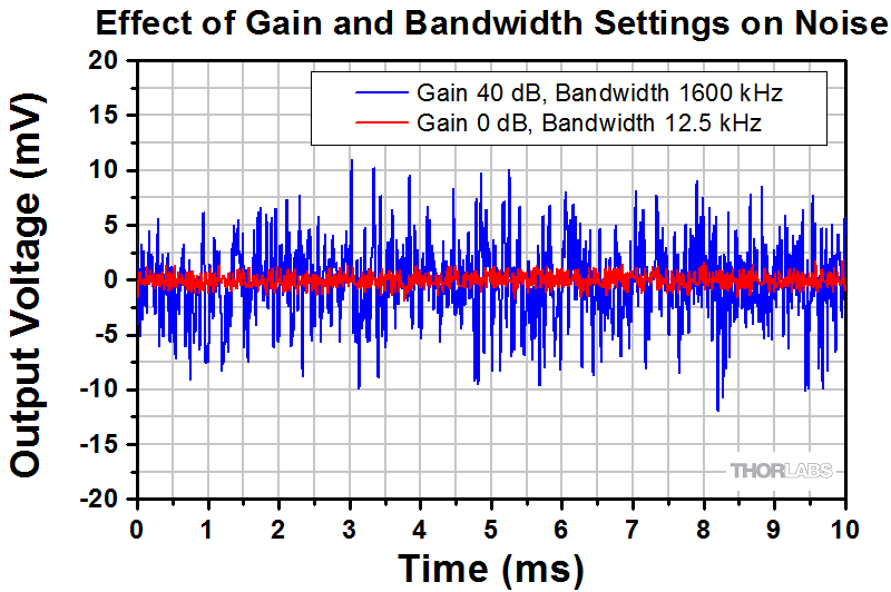
These traces compare the noise level for the lowest gain and bandwidth settings to the noise level for the highest gain and bandwidth settings.
Click to Enlarge
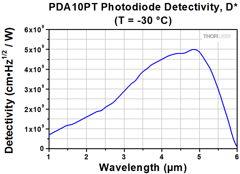
The graph above is for the 0 dB gain setting.
Detectivity, D*, is defined as:

where A is the area of the photosensitive region of the detector, Δf is the effective noise bandwidth, and NEP is the noise-equivalent power. For the PDA10PT,

For more information, please see the manual.
Output Signal
BNC Female
0 - 5 V at 50 Ω
0 - 10 V at High Z
100 mA Max Current
Power Input
4-Pin Female
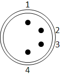
| Pin | Connection |
|---|---|
| 1 | -12 V |
| 2 | Ground |
| 3 | +5 V |
| 4 | +12 V |
Photodiode Tutorial
Theory of Operation
A junction photodiode is an intrinsic device that behaves similarly to an ordinary signal diode, but it generates a photocurrent when light is absorbed in the depleted region of the junction semiconductor. A photodiode is a fast, highly linear device that exhibits high quantum efficiency and may be used in a variety of different applications.
It is necessary to be able to correctly determine the level of the output current to expect and the responsivity based upon the incident light. Depicted in Figure 1 is a junction photodiode model with basic discrete components to help visualize the main characteristics and gain a better understanding of the operation of Thorlabs' photodiodes.
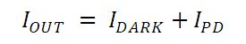
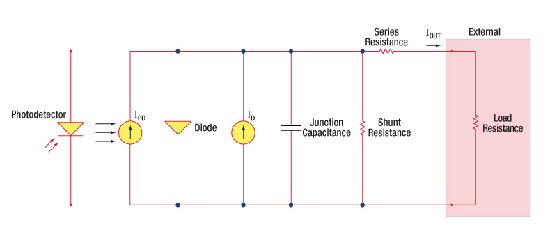
Figure 1: Photodiode Model
Photodiode Terminology
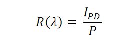
Responsivity
The responsivity of a photodiode can be defined as a ratio of generated photocurrent (IPD) to the incident light power (P) at a given wavelength:
Modes of Operation (Photoconductive vs. Photovoltaic)
A photodiode can be operated in one of two modes: photoconductive (reverse bias) or photovoltaic (zero-bias). Mode selection depends upon the application's speed requirements and the amount of tolerable dark current (leakage current).
Photoconductive
In photoconductive mode, an external reverse bias is applied, which is the basis for our DET series detectors. The current measured through the circuit indicates illumination of the device; the measured output current is linearly proportional to the input optical power. Applying a reverse bias increases the width of the depletion junction producing an increased responsivity with a decrease in junction capacitance and produces a very linear response. Operating under these conditions does tend to produce a larger dark current, but this can be limited based upon the photodiode material. (Note: Our DET detectors are reverse biased and cannot be operated under a forward bias.)
Photovoltaic
In photovoltaic mode the photodiode is zero biased. The flow of current out of the device is restricted and a voltage builds up. This mode of operation exploits the photovoltaic effect, which is the basis for solar cells. The amount of dark current is kept at a minimum when operating in photovoltaic mode.
Dark Current
Dark current is leakage current that flows when a bias voltage is applied to a photodiode. When operating in a photoconductive mode, there tends to be a higher dark current that varies directly with temperature. Dark current approximately doubles for every 10 °C increase in temperature, and shunt resistance tends to double for every 6 °C rise. Of course, applying a higher bias will decrease the junction capacitance but will increase the amount of dark current present.
The dark current present is also affected by the photodiode material and the size of the active area. Silicon devices generally produce low dark current compared to germanium devices which have high dark currents. The table below lists several photodiode materials and their relative dark currents, speeds, sensitivity, and costs.
| Material | Dark Current | Speed | Spectral Range | Cost |
|---|---|---|---|---|
| Silicon (Si) | Low | High Speed | Visible to NIR | Low |
| Germanium (Ge) | High | Low Speed | NIR | Low |
| Gallium Phosphide (GaP) | Low | High Speed | UV to Visible | Moderate |
| Indium Gallium Arsenide (InGaAs) | Low | High Speed | NIR | Moderate |
| Indium Arsenide Antimonide (InAsSb) | High | Low Speed | NIR to MIR | High |
| Extended Range Indium Gallium Arsenide (InGaAs) | High | High Speed | NIR | High |
| Mercury Cadmium Telluride (MCT, HgCdTe) | High | Low Speed | NIR to MIR | High |
Junction Capacitance
Junction capacitance (Cj) is an important property of a photodiode as this can have a profound impact on the photodiode's bandwidth and response. It should be noted that larger diode areas encompass a greater junction volume with increased charge capacity. In a reverse bias application, the depletion width of the junction is increased, thus effectively reducing the junction capacitance and increasing the response speed.
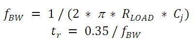
Bandwidth and Response
A load resistor will react with the photodetector junction capacitance to limit the bandwidth. For best frequency response, a 50 Ω terminator should be used in conjunction with a 50 Ω coaxial cable. The bandwidth (fBW) and the rise time response (tr) can be approximated using the junction capacitance (Cj) and the load resistance (RLOAD):
Noise Equivalent Power
The noise equivalent power (NEP) is the generated RMS signal voltage generated when the signal to noise ratio is equal to one. This is useful, as the NEP determines the ability of the detector to detect low level light. In general, the NEP increases with the active area of the detector and is given by the following equation:
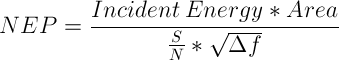
Here, S/N is the Signal to Noise Ratio, Δf is the Noise Bandwidth, and Incident Energy has units of W/cm2. For more information on NEP, please see Thorlabs' Noise Equivalent Power White Paper.
Terminating Resistance
A load resistance is used to convert the generated photocurrent into a voltage (VOUT) for viewing on an oscilloscope:
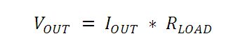
Depending on the type of the photodiode, load resistance can affect the response speed. For maximum bandwidth, we recommend using a 50 Ω coaxial cable with a 50 Ω terminating resistor at the opposite end of the cable. This will minimize ringing by matching the cable with its characteristic impedance. If bandwidth is not important, you may increase the amount of voltage for a given light level by increasing RLOAD. In an unmatched termination, the length of the coaxial cable can have a profound impact on the response, so it is recommended to keep the cable as short as possible.
Shunt Resistance
Shunt resistance represents the resistance of the zero-biased photodiode junction. An ideal photodiode will have an infinite shunt resistance, but actual values may range from the order of ten Ω to thousands of MΩ and is dependent on the photodiode material. For example, and InGaAs detector has a shunt resistance on the order of 10 MΩ while a Ge detector is in the kΩ range. This can significantly impact the noise current on the photodiode. For most applications, however, the high resistance produces little effect and can be ignored.
Series Resistance
Series resistance is the resistance of the semiconductor material, and this low resistance can generally be ignored. The series resistance arises from the contacts and the wire bonds of the photodiode and is used to mainly determine the linearity of the photodiode under zero bias conditions.
Common Operating Circuits
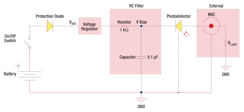
Figure 2: Reverse-Biased Circuit (DET Series Detectors)
The DET series detectors are modeled with the circuit depicted above. The detector is reverse biased to produce a linear response to the applied input light. The amount of photocurrent generated is based upon the incident light and wavelength and can be viewed on an oscilloscope by attaching a load resistance on the output. The function of the RC filter is to filter any high-frequency noise from the input supply that may contribute to a noisy output.
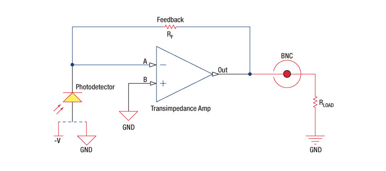
Figure 3: Amplified Detector Circuit
One can also use a photodetector with an amplifier for the purpose of achieving high gain. The user can choose whether to operate in Photovoltaic of Photoconductive modes. There are a few benefits of choosing this active circuit:
- Photovoltaic mode: The circuit is held at zero volts across the photodiode, since point A is held at the same potential as point B by the operational amplifier. This eliminates the possibility of dark current.
- Photoconductive mode: The photodiode is reversed biased, thus improving the bandwidth while lowering the junction capacitance. The gain of the detector is dependent on the feedback element (Rf). The bandwidth of the detector can be calculated using the following:
where GBP is the amplifier gain bandwidth product and CD is the sum of the junction capacitance and amplifier capacitance.
Effects of Chopping Frequency
The photoconductor signal will remain constant up to the time constant response limit. Many detectors, including PbS, PbSe, HgCdTe (MCT), and InAsSb, have a typical 1/f noise spectrum (i.e., the noise decreases as chopping frequency increases), which has a profound impact on the time constant at lower frequencies.
The detector will exhibit lower responsivity at lower chopping frequencies. Frequency response and detectivity are maximized for
![]()
| Posted Comments: | |
Martin Silies
(posted 2024-04-04 12:05:30.943) Dear Thorlabs team,
I am highly interested in the InAsSb Amplified Detector with TEC.
We plan to characterize our femtosecond laser source that is emitting light in the NIR to mid-IR spectral region.
The spectral range is ranging from 1000nm to 2300nm.
In detail, we want to implement the APD in a home-built Fourier-transform spectrometer in order to characterize the spectrum of the FemtoFiber SCIR laser.
The laser is a pulsed source emitting pulses at a repetition rate of 40MHz (pulse duration in the ps regime due to nonlinear processes).
The signal from the APD should later be fed into a PC via Analog-to-Digital Converter and the voltage from the APD should be recorded as a function of position in a Fourier-Transform spectrometer.
I am curious about the signal I would see on an oscilloscope. The bandwith of the APD is relatively narrow, hence the response time of the APD is long, right?
Would I hence only see a constant voltage signal, when the repetition rate of my laser is 40MHz?
Many thanks for your answer in advance,
Martin Silies |
The following table lists Thorlabs' selection of photodiodes, photoconductive, and pyroelectric detectors. Item numbers in the same row contain the same detector element.
| Photodetector Cross Reference | ||||||
|---|---|---|---|---|---|---|
| Wavelength | Material | Unmounted Photodiode |
Mounted Photodiode |
Biased Detector |
Amplified Detector |
Amplified Detector, OEM Package |
| 200 - 1100 nm | Si | FDS010 | SM05PD2A SM05PD2B |
DET10A2 | PDA10A2 | - |
| Si | - | SM1PD2A | - | - | - | |
| 240 - 1170 nm | B-Si | - | - | DET20X2 | - | - |
| 320 - 1000 nm | Si | - | - | - | PDA8A2 | - |
| 320 - 1100 nm | Si | FD11A | SM05PD3A | - | PDF10A2 | - |
| Si | - a | - | DET100A2 a | PDA100A2 a | PDAPC2 a | |
| 340 - 1100 nm | Si | FDS10X10 | - | - | - | - |
| 350 - 1100 nm | Si | FDS100 FDS100-CAL b |
SM05PD1A SM05PD1B |
DET36A2 | PDA36A2 | PDAPC1 |
| Si | FDS1010 FDS1010-CAL b |
SM1PD1A SM1PD1B |
- | - | - | |
| 400 - 1000 nm | Si | - | - | - | PDA015A2 FPD310-FS-VIS FPD310-FC-VIS FPD510-FC-VIS FPD510-FS-VIS FPD610-FC-VIS FPD610-FS-VIS |
- |
| 400 - 1100 nm | Si | FDS015 c | - | - | - | - |
| Si | FDS025 c FDS02 d |
- | DET02AFC(/M) DET025AFC(/M) DET025A(/M) DET025AL(/M) |
- | - | |
| 400 - 1700 nm | Si & InGaAs | DSD2 | - | - | - | - |
| 500 - 1700 nm | InGaAs | - | - | DET10N2 | - | - |
| 0.6 - 16 µm | LiTaO3 | - | - | - | PDA13L2e | - |
| 750 - 1650 nm | InGaAs | - | - | - | PDA8GS | - |
| 800 - 1700 nm | InGaAs | FGA015 | - | - | PDA015C2 | - |
| InGaAs | FGA21 FGA21-CAL b |
SM05PD5A | DET20C2 | PDA20C2 PDA20CS2 |
- | |
| InGaAs | FGA01 c FGA01FC d |
- | DET01CFC(/M) | - | - | |
| InGaAs | FDGA05 c | - | - | PDA05CF2 | - | |
| InGaAs | - | - | DET08CFC(/M) DET08C(/M) DET08CL(/M) |
- | - | |
| InGaAs | - | - | - | PDF10C2 | - | |
| 800 - 1800 nm | Ge | FDG03 FDG03-CAL b |
SM05PD6A | DET30B2 | PDA30B2 | - |
| Ge | FDG50 | - | DET50B2 | PDA50B2 | - | |
| Ge | FDG05 | - | - | - | - | |
| 900 - 1700 nm | InGaAs | FGA10 | SM05PD4A | DET10C2 | PDA10CS2 | - |
| 900 - 2600 nm | InGaAs | FD05D | - | DET05D2 | - | - |
| FD10D | - | DET10D2 | PDA10D2 | - | ||
| 950 - 1650 nm | InGaAs | - | - | - | FPD310-FC-NIR FPD310-FS-NIR FPD510-FC-NIR FPD510-FS-NIR FPD610-FC-NIR FPD610-FS-NIR |
- |
| 1.0 - 5.8 µm | InAsSb | - | - | - | PDA10PT(-EC) | - |
| 2.0 - 8.0 µm | HgCdTe (MCT) | VML8T0 VML8T4 f |
- | - | PDAVJ8 | - |
| 2.0 - 10.6 µm | HgCdTe (MCT) | VML10T0 VML10T4 f |
- | - | PDAVJ10 | - |
| 2.7 - 5.0 µm | HgCdTe (MCT) | VL5T0 | - | - | PDAVJ5 | - |
| 2.7 - 5.3 µm | InAsSb | - | - | - | PDA07P2 | - |
| Item # | PDA10PT(-EC) |
|---|---|
| Click Image to Enlarge | 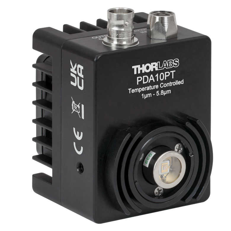 |
| Detector Element (Click for Image) |
InAsSb |
| Wavelength Range | 1.0 - 5.8 µm |
| Peak Wavelength (λP) | 4.9 µm |
| Peak Responsivity | 0.8 A/W (Min) at λP 1.6 A/W (Typ.) at λP |
| Active Area | Ø1 mm |
| Window Material | Sapphire |
| Gain Settings | 8 Steps: 0, 4, 10, 16, 22, 28, 34, or 40 dB |
| Bandwidth Settings | 8 Steps from 12.5 kHz to 1600 kHz |
| Noise-Equivalent Power (NEP) | 1.49 x 10⁻¹⁰ W/Hz1/2 (for 40 dB Gain and 1600 kHz Bandwidth) |
- Sensitive to Chopped or Pulsed Mid-IR Light from 1.0 µm to 5.8 µm
- Detector is Cooled to -30 °C to Reduce Thermal Noise
- Ø1 mm Active Area
- Variable Gain Amplifier (100 V/A to 10 000 V/A)
- Variable Bandwidth (12.5 kHz to 1600 kHz)
- Internal SM1 (1.035"-40) Threading
- Location-Specific Power Adapter Included