Piezoelectric Deformable Mirrors
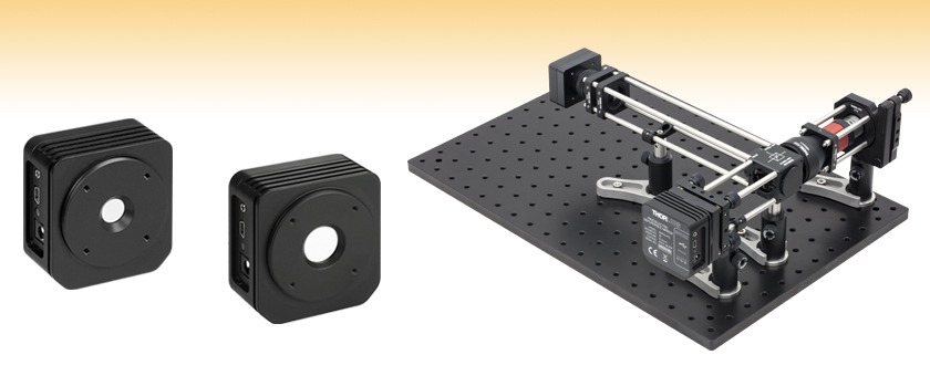
- 40-Actuator Array for Correcting Aberrations
- Built-In High-Voltage Driver
- Open- or Closed-Loop Operation
DMP40-F01
Deformable Mirror with Tip-Tilt Actuation and UV-Enhanced Aluminum Coating for 250 to 450 nm
DMH40-P01
High-Stroke Deformable Mirror with Protected Silver Coating for 450 nm to 20 µm
Application Idea
DMP40-P01 Protected Silver Coated DM Integrated into an AO System.
See the Application Idea tab for details.

Please Wait
Features
- Controllable Wavefront Correction
- High Reflectance Metallic Mirror Coatings Available from Stock:
- UV-Enhanced Aluminum (250 - 450 nm)
- Protected Silver (450 nm - 20 µm)
- Single-Wavelength Crystalline Coatings Available for 900 nm to 5.0 µm via Tech Support
- Two Deformable Mirror Types Available:
- Ø10 mm Pupil with Tip/Tilt Actuation
- Ø14 mm Pupil with High Stroke
- Mirror is Deformed by 40 Electrodes Attached to a Single Piezoceramic Disk (See Diagrams Below)
- 4 kHz Max Update Rate
- Built-In High-Voltage Driver
- Software Program for Mirror Control via USB 2.0 Interface
- Compact 64.0 mm x 60.0 mm x 30.9 mm (2.52" x 2.36" x 1.22") Housing
Thorlabs' Piezoelectric Deformable Mirrors provide fast, responsive platforms for changing optical wavefronts, making them ideal for correcting distortions that result from common sources of wavefront aberrations, such as astigmatism and coma (see the Types of Aberrations tab for more details). Each mirror can be controlled manually using the included software or used in a closed-loop system with a Thorlabs' Shack-Hartmann wavefront sensor (see the Software tab for more details).
We offer two varieties of deformable mirror. Our DMP40 series features a mirror with a Ø10 mm pupil suspended by biomorph benders. These benders enable tip/tilt actuation and allow the mirrors to be precisely aligned. The mirror used in the DMH40 series has a larger, Ø14 mm pupil, but lacks tip/tilt biomorph benders. In addition, the actuators found on the DMH40 series offer more than twice the physical stroke compared to those on our DMP40 series. Each of these mirrors is available from stock with one of two optical coatings: UV-enhanced aluminum for 250 to 450 nm or protected silver for 450 nm to 20 µm (see the Specs and Graphs tabs for performance data). For applications using high power or requiring higher reflectance, these mirrors can be customized with the crystalline coatings in use on our supermirrors. Please contact Tech Support for more information.
The front plate of each deformable mirror housing has external SM2 (2.035"-40) threads for compatibility with Thorlabs' SM2-threaded lens tubes and has four 4-40 taps that are compatible with Thorlabs' 30 mm cage systems. Each mirror is shipped with an SM2CP1 end cap to protect the mirror surface when not in use, a power supply with a location-specific power cord, USB 2.0 cable for connecting the mirror to a PC, a calibration certificate, and a quick start guide. The complete manual can be downloaded by clicking on the red document icon (![]() ) next to any of the part numbers below. The control software is available for download from the Software tab.
) next to any of the part numbers below. The control software is available for download from the Software tab.
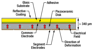
Click to Enlarge
A schematic showing the internal structure of the deformable mirror.
Principle of Operation
To construct the mirror assembly, a thin glass disk coated with UV-enhanced aluminum or protected silver is glued to a circular piezoceramic disk. The electrode attached to the back of the disk is divided into 40 single segments arranged in a circular keystone pattern. See the Graphs tab for the reflectance of the available coatings, the drawings below for diagrams of the keystone patterns, and the drawing to the right for a diagram of the mirror/piezoceramic disk/electrode structure.
Each segment is controlled independently by applying a positive voltage. The surface is designed to be flat when half of the maximum voltage is applied across each electrode (see the drawing to the lower right). Pure spherical shapes can be generated by applying no voltage or the maximum voltage. A lower voltage at one electrode will result in a locally concave mirror shape, while a higher voltage will result in a locally convex mirror shape.

Click to Enlarge
This drawing shows the response of a single segment of the deformable mirror different voltages.
In addition to the 40 actuators, our DMP40 series of mirrors have three bimorph arms provide tip/tilt adjustment. The top layer of each arm is part of the ceramic disk carrying the actuators and only connects to the main part of disk via a small connection point. The end of the arm is attached to a carrier board. A second piezoelectric layer is bonded to the bottom of each arm, configured so that one layer will shrink while the other expands as an applied voltage is increased. Applying a voltage to an arm will change the height of the mirror at the connection point. By using three mechanically identical arms, the mirror can be tilted in any direction over a ±2 mrad range (see the Specs tab). Applying the same voltage to each arm will move the mirror parallel to its surface while holding the tilt constant, which can be used for optical phase modulation.
To effectively use the deformable mirror in an adaptive optics application, the input beam must fill or overfill the pupil diameter of the deformable mirror (matching the 1/e² beam diameter to the pupil diameter is a common practice), and the defined pupil in the software for the wavefront sensor needs to be adjusted to match the pupil of the deformable mirror.
For more information on choosing the type of deformable mirror that is best for your application, please see the Selecting a DM tab.
All technical data are valid at 23 ± 5 °C and 45 ± 15% relative humidity (non-condensing).
| Item # Prefix | DMP40(/M) | DMH40(/M) | |
|---|---|---|---|
| Actuators | |||
| Number of Segments in Piezoceramic Disk |
40 Total (Elements 1 - 24 Inside Pupil Diameter, Elements 25 - 40 Outside Pupil Diameter) |
||
| Tip/Tilt | 3 Spiral Arms | N/A | |
| Segment Voltage Range | 0 to +200 V (Default: +100 V for Flat Mirror) |
0 to +300 V (Default: +150 V for Flat Mirror) |
|
| Tip/Tilt Arm Voltage Range | 0 to +200 V (Default: +100 V for Non-Tilted Mirror) | N/A | |
| Tip/Tilt Range | ±2.0 mrada | N/A | |
| Hysteresis of Piezoceramic Materialb |
15% Typical, 25% Max | 20% Typical, 25% Max | |
| Optical | |||
| Optical Aperturec | Ø11.5 mm | Ø17.0 mm | |
| Pupil Diameterc | 10.0 mm | 14.0 mm | |
| Surface Flatness (RMS) | 100 nm (Defocus Term Actively Flattened) |
200 nm (Defocus Term Actively Flattened) |
|
| Dynamical | |||
| Pattern Update Rate (Max) | 4 kHz via USB 2.0 (Over Entire Voltage Range) | ||
| Mirror Response Time | 0.5 ms (Full Stroke) | ||
| Tip/Tilt Response Time | 5 ms (Full Stroke) | N/A | |
| Interfaces | |||
| PC Interfaced | High-Speed USB 2.0 (USB 1.1 Compatible), Mini USB Connector |
||
| Analog Feedback Inputd | 2.5 mm Stereo Plug Current: 1 nA - 10 mA, Voltage: 0 - 2.5 V |
||
| General | |||
| Operating Temperature Range | +5 to +35 °C (Non-Condensing) | ||
| Storage Temperature Range | -20 °C to +70 °C | ||
| Operating Altitude | 3000 m (Maximum) | ||
| Housing Dimensions (H x W x D) |
64.0 mm x 60.0 mm x 30.9 mm (2.52" x 2.36" x 1.22") |
||
| Weight | 0.18 kg (0.4 lbs) | ||
| Mounting Options | |||
| Cage Systems | 30 mm Cage Compatible via Four 4-40 Taps | ||
| Lens Tubes | Front Plate with External SM2 (2.035"-40) Threads | ||
| Post | 8-32 and 1/4"-20 (M4 and M6) Taps on the Bottom of the Housing |
||
| Power | |||
| Power Supply | 12 V DC, 18 VA | ||
| Item # Prefix | DMP40(/M) | DMH40(/M) | |
|---|---|---|---|
| Aberration | Zernike Coefficient |
Physical Strokea | |
| Defocus | Z5 | ±6.5 µm | ±17.6 µm |
| Astigmatism | Z4, Z6 | ±6.8 µm | ±18.4 µm |
| Coma | Z8, Z9 | ±2.5 µm | ±6.8 µm |
| Trefoil | Z7, Z10 | ±2.4 µm | ±6.5 µm |
| Tetrafoil | Z11, Z15 | ±2.1 µm | ±5.7 µm |
| Secondary Astigmatism |
Z12, Z14 | ±1.1 µm | ±3.0 µm |
| Third Order Spherical Aberration |
Z13 | ±1.0 µm | ±2.7 µm |
| Reflective Coating Specifications | |||
|---|---|---|---|
| Item # Suffix | -F01 | -P01 | |
| Coating | UV Enhanced Aluminum | Protected Silver | |
| Average Reflectance (Click for Graph)a |
>89% (250 - 450 nm) | >97.5% (450 nm - 2 µm) >96% (2 - 20 µm) |
|
| Damage Thresholdb | CW | 1 W/cm (250 - 450 nm) |
4 W/cm (450 nm - 2 µm) |
| Pulsed | 0.2 J/cm² (355 nm, 10 ns, 10 Hz, Ø0.38 mm) | 1 J/cm² (1064 nm, 10 ns, 10 Hz, Ø10 mm) | |
Deformable Mirror Hysteresis
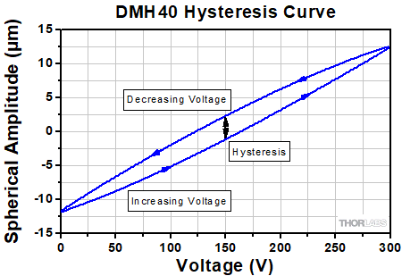
Click to Enlarge
This graph shows a typical hysteresis curve for a DMH40 mirror undergoing spherical deformation as the voltage across all 40 mirror segments is cycled between 0 and 300 V. The hysteresis is indicated by the black line in the graph above.
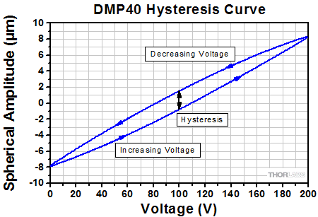
Click to Enlarge
This graph shows a typical hysteresis curve for a DMP40 mirror undergoing spherical deformation as the voltage across all 40 mirror segments is cycled between 0 and 200 V. The hysteresis is indicated by the black line in the graph above.
HR Coating Reflectance
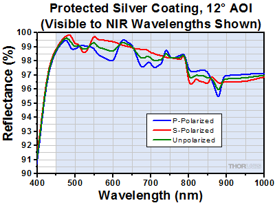
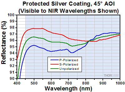
The blue shaded regions denote the reflection bands for which the performance is guaranteed to meet the stated specifications. Performance outside the shaded regions will vary from lot to lot and is not guaranteed.
UV-Enhanced Aluminum (Item #s Ending in -F01)
Protected Silver (Item #s Ending in -P01)
Click to Enlarge
Excel Spreadsheet with Raw Data for Protected Silver
Protected silver coating reflectance from 450 nm to 1 µm at 12° AOI. The coating is designed for use from 450 nm to 20 µm.
Click to Enlarge
Excel Spreadsheet with Raw Data for Protected Silver
Protected silver coating reflectance from 450 nm to 1 µm at 45° AOI. The coating is designed for use from 450 nm to 20 µm.
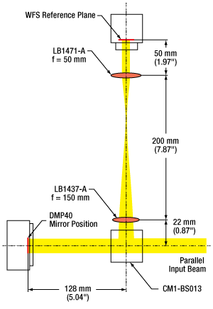
Simplified Diagram of the AO System Shown to the Left
DMP40-P01 Deformable Mirror with a Shack-Hartmann Wavefront Sensor
The sample setup below uses a Shack-Hartmann Wavefront Sensor (WFS) to measure the change in wavefront produced by a DMP40-P01 Deformable Mirror (DM). This setup was designed to help users familiarize themselves with the behavior of the DMP40 deformable mirrors, and not to provide a fully operational adaptive optics system. See the table for a list of the parts used in the system below. If you hover over a component in the image below, the corresponding item will be highlighted in the table below.
To build the system into an experimental setups for adaptive optics applications, the input collimator can be replaced with a user-supplied beam and/or a second beamsplitter can be placed just before the WFS to redirect some of the light to an experimental setup.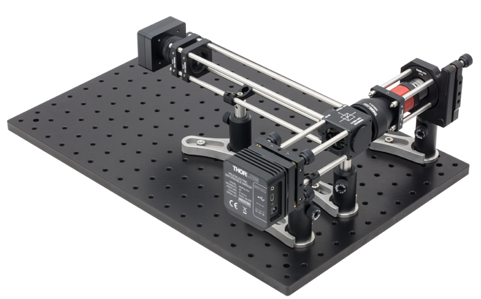
| Parts Lista | |||||
|---|---|---|---|---|---|
| Product Description | Item # | Qty. | |||
| Imperial | Metric | ||||
| Piezoelectric Deformable Mirror | DMP40-P01 | DMP40/M-P01 | 1 | ||
| Fast Shack-Hartmann Wavefront Sensor, Chrome-Masked Microlens Array, 300 - 1100 nm |
WFS20-5C | WFS20-5C/M | 1 | ||
| 3X Achromatic Galilean Beam Expander, AR Coated: 400 - 650 nm |
GBE03-A | 1 | |||
| Ø1" Protected Silver Mirrorb | PF10-03-P01 | 1 | |||
| Ø1" Biconvex Lens, 350 - 700 nmc | f = 150 mm | LB1437-A | 1 | ||
| Ø1" Biconvex Lens, 350 - 700 nmc | f = 50 mm | LB1471-A | 1 | ||
| Cage Assembly Rod | L = 1.0", 4 Pack | ER1-P4 | 1 | ||
| Cage Assembly Rod | L = 3.0", 4 Pack | ER3-P4 | 1 | ||
| Cage Assembly Rod | L = 4.0", 4 Pack | ER4-P4 | 1 | ||
| Cage Assembly Rod | L = 8.0", 4 Pack | ER8-P4 | 1 | ||
| SM1 Lens Tube | 0.3" Thread Depth | SM1L03 | 2 | ||
| SM1 Lens Tubeb | 1.0" Thread Depth | SM1L10 | 1 | ||
| SM1 Lens Tubeb | 4.0" Thread Depth | SM1L40 | 1 | ||
| Pedestal Post Holder | L = 2.19" (54.7 mm) | PH2E | PH50E/M | 4 | |
| Ø1/2" Stainless Steel Postd | L = 1.5" (40 mm) | TR1.5 | TR40/M | 1 | |
| Ø1/2" Stainless Steel Post | L = 2.0" (50 mm) | TR2 | TR50/M | 3 | |
| Small Clamping Fork, 1.25" | CF125 | 4 | |||
| Parts Lista | |||
|---|---|---|---|
| Product Description | Item # | Qty. | |
| Imperial | Metric | ||
| SM1-Threaded Adapter for Ø15 mm Cylindrical Componentse |
AD15F | 1 | |
| Fiber-Coupled Laser Source, 635 nmf | S1FC635 | 1 | |
| Single Mode Fiber Patch Cablef | P1-630A-FC-1 | 1 | |
| Cube-Mounted, Non-Polarizing 50:50 Beamsplitter | CCM1-BS013 | CCM1-BS013/M | 1 |
| SM1-Threaded 30 mm Cage Plate | CP33 | CP33/M | 2 |
| 30 mm Cage Adapter | CP33B | 2 | |
| Ø2" Round Cage Plate | CP38 | 1 | |
| Cage System Alignment Plate with Ø0.9 mm Holeg | CPA1 | 2 | |
| 635 nm FC/PC Collimation Package | F810FC-635 | 1 | |
| Cage-Compatible Kinematic Mount for Ø1" Optic | KC1T | KC1T/M | 1 |
| Kinematic Mount for Ø2" Optic | KM200 | 1 | |
| 30 mm Cage Plate with Ø1.2" Double Bore | CP36 | 1 | |
| Ø25 mm Absorptive ND Filter, OD = 1.0h | NE10A | 1 | |
| Thread Adapter, External SM1 to Internal SM2i | SM1A2 | 1 | |
| Thread Adapter, External C-Mount to Internal SM1 | SM1A9 | 1 | |
| End Cap, Externally SM1-Threaded | SM1CP2 | 1 | |
| SM1 Coupler, External Threadsj | SM1T2 | 1 | |
| Anodized Aluminum Breadboard, 12" x 18" x 1/2" (300 mm x 450 mm x 12.7 mm), 1/4"-20 (M6) Taps |
MB1218 | MB3045/M | 1 |
A software package with a graphical user interface for operating the DMP40 or DMH40 deformable mirrors for adaptive optics applications can be downloaded using the link below. Driver packages are included for developers who want to extend or adapt the functionality of the device with custom applications.
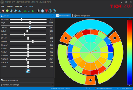
Click to Enlarge
A screenshot of the DMP40 deformable mirror software GUI.
Software and GUI Features
Display/Output Options
- Numerical and Graphical Mirror Segment and Tilt Element Voltage Control
- Voltage Pattern Generation Using Single or Grouped Segments
- Integrated Hysteresis Compensation
- Save and Load User-Defined Patterns
- Adjust Tilt by Altitude and Amplitude Angle
- Pre-Defined Zernike Function Pattern
- Integrated Adaptive Optics Control Loop Using Feedback from Thorlabs' Wavefront Sensors
- Analog Voltage and Current Inputs for Feedback
Drivers
The software includes a driver package for constructing custom applications with the following software packages:
- C Compilers
- LabWindows™/CVI
- LabVIEW™
- .NET
Ideally, an optical image-forming system will produce a unique image point for each object point. Any departures from this ideal theory of Gaussian (also known as paraxial or first-order) Optics are known as aberrations and can be categorized into two main types: monochromatic (single color) aberrations and chromatic (varying wavelength) aberrations. When aberrations are present, the peak intensity will be reduced and the image or laser beam propagating to a target will be blurred. Below, we will take a look at the seven primary types of aberrations, five of which are of the monochromatic variety and two of which are of the chromatic variety. Deformable mirrors are capable of removing all types of monochromatic aberrations from a wavefront to allow for the formation of an ideal, diffraction-limited image, even if optics without diffraction-limited performance are being used in the optical system.
Monochromatic Aberrations
There are five primary monochromatic aberrations, which can be further divided into two subgroups: those that deteriorate the image (spherical aberration, coma, and astigmatism) and those that deform the image (field curvature and distortion). These aberrations are a direct result of departures from first-order (i.e., sinθ≈θ) theory, which assumes the light rays make small angles with the principal axis. As soon as one wants to consider light rays incident on the periphery of a lens, the statement sinθ≈θ, which forms the basis of paraxial optics, is no longer satisfactory and one must consider more terms in the expansion:

The five primary monochromatic aberrations were first studied by Ludwig von Seidel, and hence, they are frequently referred to as the Seidel aberrations. Please note that since the expansion of sinθ is an infinite sum, the five monochromatic aberrations discussed below are not the only ones possible; there are additional higher-order aberrations that make smaller contributions to image degradation. The surface of the deformable mirror can be altered to accommodate all of these types of monochromatic aberrations.
For parallel incoming light rays, an ideal lens will be able to focus the rays to a point on the optical axis as shown in Fig. 1a; consequently, under ideal circumstances, the image of a point source that is located on the optical axis will be a bright circular disk surrounded by faint rings (see the Airy diffraction pattern shown in Fig. 1b). However, in reality, the light rays that strike a spherical converging lens far from the principal axis will be focused to a point that is closer to the lens than those light rays that strike the spherical lens near the principal axis (see Fig. 1c). Consequently, there is no single focus for a spherical lens, and the image will appear to be blurred; instead of having an Airy diffraction pattern in which nearly all the light is contained in a central bright circular spot, spherical aberration will redistribute some of the light from the central disk to the surrounding rings (see Fig. 1d), thereby reducing image contrast. Whenever spherical aberration is present, the best focus for an uncorrected lens will be somewhere between the focal planes of the peripheral and axial rays. Please note that spherical aberration only pertains to object points that are located on the optical axis.

Figure 1. Comparison of an ideal situation to one in which spherical aberration is present. (a) For a perfect lens, all incoming light rays get focused to a single point. (b) The Airy diffraction pattern corresponding to a point source that has been imaged by a perfect lens consists of a bright central spot surrounded by faint concentric rings. (c) For a real lens, light incident on the edges of a lens is refracted more than the light striking the center of the lens, and thus, there is not one unique focal point for all incident light rays. (d) Spherical aberration degrades resolution by redistributing some of the light from the central bright spot to the surrounding concentric rings.
Coma, or comatic aberration, is an image-degrading aberration associated with object points that are even slightly off axis. When an off-axis bundle of light is incident on a lens, the light will undergo different amounts of refraction depending on where it strikes the lens (see Fig. 2a); as a result, each annulus of light will focus onto the image plane at a slightly different height and with a different spot size (see Fig. 2b), thereby leading to different transverse magnifications. The resulting image of a point source, which is shown in Fig. 2c, is a complicated asymmetrical diffraction pattern with a bright central core and a triangular flare that departs drastically from the classical Airy pattern shown in Fig 1b above. The elongated comet-like structure from which this type of aberration takes its name can extend either towards or away from the optical axis depending on whether the comatic aberration is negative or positive, respectively. Due to the asymmetry that coma causes in images, many consider it to be the worst type of aberration.

Figure 2. The effects of positive coma are shown. (a) When a light source is off-axis, the various portions of the lens do not refract the light to the same point on the image plane. (b) The central region of the lens forms a point image at the vertex of the cone, while larger rings on the periphery of the lens correspond to larger comatic circles that are displaced farther from the principal axis. (c) Coma leads to a complicated asymmetrical comet-like diffraction pattern characterized by an elongated structure of blotches and arcs. Note that the diffraction pattern shown assumes no spherical aberration.
Astigmatism, like coma, is an aberration that arises when an object point is moved away from the optical axis. Under such conditions, the incident cone of light will strike the lens obliquely, leading to a refracted wavefront characterized by two principal curvatures that ultimately determine two different focal image points. Figure 3a shows the two planes one needs to consider: the tangential (also known as the meridional) plane and the sagittal plane; the tangential plane is defined by the chief ray (i.e., the light ray from the object that passes through the center of the lens) and the optical axis, while the sagittal plane is a plane that contains the chief ray and is perpendicular to the tangential plane. In addition to the chief light ray, Fig. 3a also shows two other off-axis light rays, one passing through the tangential plane and the other passing through the sagittal plane. For complex multi-element lens systems (e.g., microscope objective or ASOM system), the tangential plane remains coherent from one end of the system to the other while the sagittal plane usually changes slope as the chief ray’s propagation direction is altered by the various components in the lens system. Consequently, in general, the focal lengths associated with these planes will be different (see Fig. 3b). If the sagittal focus and the tangential focal points are coincident, then the object point is on axis and the lens is free of astigmatism. However, as the amount of astigmatism present increases, the distance between these two foci will also increase, and as a result, the image will lose definition around its edges. The presence of astigmatism will cause the ideal circular point image to be blurred into a complicated elongated diffraction pattern that appears more linelike when more astigmatism is present (see Figs. 3c and 3d).

Figure 3. The effects of astigmatism, assuming the absence of spherical aberration and coma, are illustrated. (a) The tangential and sagittal planes are shown. (b) Light rays in the tangential and sagittal planes are refracted differently, ultimately leading to two different focal planes, which are labeled as the tangential focus and sagittal focus. (c) The Airy diffraction pattern of a point source as viewed at the tangential focal plane. (d) The Airy diffraction pattern of a point source as viewed at the sagittal focal plane.
For most optical systems, the final image must be formed on a planar surface; however, in actuality, a lens that is free of all other off-axis aberrations creates an image on a curved surface known as a Petzval surface. This nominal curvature of this surface, which is known as the Petzval curvature, is the reciprocal of the lens radius. For a positive lens, this surface curves inward towards the object plane, whereas for a negative lens, the surface curves away from that plane. The field curvature aberration arises from forcing a naturally curved image surface into a flat one. For the image, the presence of field curvature makes it impossible to have both the edges and central region of the image be crisp simultaneously. If the focal plate is shifted to the vertex of the Petzval surface (Position A in Fig. 4), the central part of the image will be in focus while the outer portion of the image will be blurred, making it impossible to distinguish minor structural details in this outer region. Alternatively, if the image plane is moved to the edges of the Petzval surface (Position B in Fig. 4), the opposite effect occurs; the edges of the image will come into focus, but the central region will become blurred. The best compromise between these two extremes is to place the image plane somewhere in between the vertex and edges of the Petzval surface, but regardless of its location, the image will never appear sharp and crisp over the entire field of view.

Figure 4. Field curvature, an aberration associated with off-axis objects, arises because the best image is not formed on the paraxial image plane but on a parabolic surface called the Petzval surface. (a) Depending on the location of the focal plane along the optic axis, either the central (if at location A) or peripheral (if at location B) portions of the field of view will be in focus but not both. (b) The central portion of the image will be crisp if the image plane is located at position A. (c) The edges of the image will be sharply in focus if the image plane is located at position B.
The last of the Seidel aberrations is distortion, which is easily recognized in the absence of all other monochromatic aberrations because it deforms the entire image even though each point is sharply focused. Distortion arises because different areas of the lens usually have different focal lengths and magnifications. If no distortion is present in a lens system, the image will be a true magnified reproduction of the object (see Fig. 5b). However, when distortion is present, off-axis points are imaged either at a distance greater than normal or less than normal, leading to a pincushion (see Fig. 5a) or barrel (see Fig. 5c) shape, respectively.
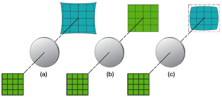
Figure 5. The effects of distortion, assuming the absence of all other forms of aberration, are illustrated. (a) Positive or pincushion distortion occurs when the transverse magnification of a lens increases with the axial distance; this effect causes each image point to be displaced radially outward from the center, with the most distant points undergoing the largest displacements. (b) If no distortion is present, the image will be a scaled duplicate of the object. (c) Negative or barrel distortion occurs when the transverse magnification of a lens decreases with axial distance; in this case, each image point moves radially inward toward the center; again, the most distant points undergo the largest displacements.
Chromatic Aberrations
The monochromatic aberrations discussed above can all be compensated for using a deformable mirror such as the one included in these adaptive optics kits. However, when a broadband light source is used, chromatic aberrations will result. Since a DM cannot compensate for these aberrations, we will only briefly mention them here. Chromatic aberrations, which come in two forms (i.e., lateral and longitudinal), arise from the variation of the index of refraction of a lens with incident wavelength. Since blue light is refracted more than red light, the lens is not capable of focusing all colors to the same focal point; therefore, the image size and focal point for each color will be slightly different, leading to an image that is surrounded by a halo. Generally, since the eye is most sensitive to the green part of the spectrum, the tendency is to focus the lens for that region; if the image plane is then moved towards (away from) the lens, the periphery of the blurred image will be tinted red (blue).
Introduction:
Adaptive optics (AO) is a rapidly growing multidisciplinary field encompassing physics, chemistry, electronics, and computer science. AO systems are used to correct (shape) the wavefront of a beam of light. Historically, these systems have their roots in the international astronomy and US defense communities. Astronomers realized that if they could compensate for the aberrations caused by atmospheric turbulence, they would be able to generate high resolution astronomical images; with sharper images comes an additional gain in contrast, which is also advantageous for astronomers since it means that they can detect fainter objects that would otherwise go unnoticed. While astronomers were trying to overcome the blurring effects of atmospheric turbulence, defense contractors were interested in ensuring that photons from their high-power lasers would be correctly pointed so as to destroy strategic targets. More recently, due to advancements in the sophistication and simplicity of AO components, researchers have utilized these systems to make breakthroughs in the areas of femtosecond pulse shaping, microscopy, laser communication, vision correction, and retinal imaging. Although dramatically different fields, all of these areas benefit from an AO system due to undesirable time-varying effects.
Typically, an AO system is comprised from three components: (1) a wavefront sensor, which measures these wavefront deviations, (2) a deformable mirror, which can change shape in order to modify a highly distorted optical wavefront, and (3) real-time control software, which uses the information collected by the wavefront sensor to calculate the appropriate shape that the deformable mirror should assume in order to compensate for the distorted wavefront. Together, these three components operate in a closed-loop fashion. By this, we mean that any changes caused by the AO system can also be detected by that system. In principle, this closed-loop system is fundamentally simple; it measures the phase as a function of the position of the optical wavefront under consideration, determines its aberration, computes a correction, reshapes the deformable mirror, observes the consequence of that correction, and then repeats this process over and over again as necessary if the phase aberration varies with time. Via this procedure, the AO system is able to improve optical resolution of an image by removing aberrations from the wavefront of the light being imaged.
The Wavefront Sensor:
The role of the wavefront sensor in an adaptive optics system is to measure the wavefront deviations from a reference wavefront. There are three basic configurations of wavefront sensors available: Shack-Hartmann wavefront sensors, shearing interferometers, and curvature sensors. Each has its own advantages in terms of noise, accuracy, sensitivity, and ease of interfacing it with the control software and deformable mirror. Of these, the Shack-Hartmann wavefront sensor has been the most widely used.
A Shack-Hartmann wavefront sensor uses a lenslet array to divide an incoming beam into a bunch of smaller beams, each of which is imaged onto a CCD camera, which is placed at the focal plane of the lenslet array. If a uniform plane wave is incident on a Shack-Hartmann wavefront sensor (refer to Fig. 1), a focused spot is formed along the optical axis of each lenslet, yielding a regularly spaced grid of spots in the focal plane. However, if a distorted wavefront (i.e., any non-flat wavefront) is used, the focal spots will be displaced from the optical axis of each lenslet. The amount of shift of each spot’s centroid is proportional to the local slope (i.e., tilt) of the wavefront at the location of that lenslet. The wavefront phase can then be reconstructed (within a constant) from the spot displacement information obtained (see Fig. 2).

Figure 1. When a planar wavefront is incident on the Shack-Hartmann wavefront sensor's microlens array, the light imaged on the CCD sensor will display a regularly spaced grid of spots. If, however, the wavefront is aberrated, individual spots will be displaced from the optical axis of each lenslet; if the displacement is large enough, the image spot may even appear to be missing. This information is used to calculate the shape of the wavefront that was incident on the microlens array.
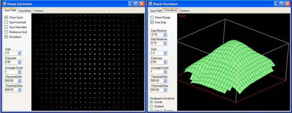
Figure 2. Two Shack-Hartmann wavefront sensor screen captures are shown: the spot field (left-hand frame) and the calculated wavefront based on that spot field information (right-hand frame).
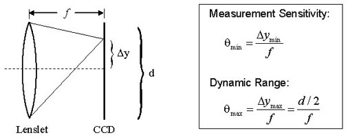
Figure 3. Dynamic range and measurement sensitivity are competing properties of a Shack-Hartmann wavefront sensor. Here, f, Δy, and d represent the focal length of the lenslet, the spot displacement, and the lenslet diameter, respectively. The equations provided for the measurement sensitivity θ min and the dynamic range θmax are obtained using the small angle approximation. θmin is the minimum wavefront slope that can be measured by the wavefront sensor. The minimum detectable spot displacement Δymin depends on the pixel size of the photodetector, the accuracy of the centroid algorithm, and the signal to noise ratio of the sensor. θmax is the maximum wavefront slope that can be measured by the wavefront sensor and corresponds to a spot displacement of Δymax, which is equal to half of the lenslet diameter. Therefore, increasing the sensitivity will decrease the dynamic range and vice versa.
The four parameters that greatly affect the performance of a given Shack-Hartmann wavefront sensor are the number of lenslets (or lenslet diameter, which typically ranges from ~100 – 600 μm), dynamic range, measurement sensitivity, and the focal length of the lenslet array (typical values range from a few millimeters to about 30 mm). The number of lenslets restricts the maximum number of Zernike coefficients that a reconstruction algorithm can reliably calculate; studies have found that the maximum number of coefficients that can be used to represent the original wavefront is approximately the same as the number of lenslets. When selecting the number of lenslets needed, one must take into account the amount of distortion s/he is trying to model (i.e., how many Zernike coefficients are needed to effectively represent the true wave aberration). When it comes to measurement sensitivity θmin and dynamic range θmax, these are competing specifications (see Fig. 3 to the right). The former determines the minimum phase that can be detected while the latter determines the maximum phase that can be measured.
A Shack-Hartmann sensor’s measurement accuracy (i.e., the minimum wavefront slope that can be measured reliably) depends on its ability to precisely measure the displacement of a focused spot with respect to a reference position, which is located along the optical axis of the lenslet. A conventional algorithm will fail to determine the correct centroid of a spot if it partially overlaps another spot or if the focal spot of a lenslet falls outside of the area of the sensor assigned to detect it (i.e., spot crossover). Special algorithms can be implemented to overcome these problems, but they limit the dynamic range of the sensor (i.e., the maximum wavefront slope that can be measured reliably). The dynamic range of a system can be increased by using a lenslet with either a larger diameter or a shorter focal length. However, the lenslet diameter is tied to the needed number of Zernike coefficients; therefore, the only other way to increase the dynamic range is to shorten the focal length of the lenslet, but this in turn, decreases the measurement sensitivity. Ideally, choose the longest focal length lens that meets both the dynamic range and measurement sensitivity requirements.
The Shack-Hartmann wavefront sensor is capable of providing information about the intensity profile as well as the calculated wavefront. Be careful not to confuse these. The left-hand frame of Fig. 4 shows a sample intensity profile, whereas the right-hand frame shows the corresponding wavefront profile. It is possible to obtain the same intensity profile from various wavefunction distributions.

Figure 4. Several pieces of information are provided by the Shack-Hartmann wavefront sensor, including information about the total power at each lenslet and the calculated wavefront distribution present. Here, the left-hand frame shows a sample intensity profile, while the right-hand frame shows the corresponding wavefront.
The Deformable Mirror:
The deformable mirror (DM) changes shape in response to position commands in order to compensate for the aberrations measured by the Shack-Hartmann wavefront sensor (refer to the Aberrations tab to learn more about the aberrations that the DM can correct). Ideally, it will assume a surface shape that is conjugate to the aberration profile (see Fig. 5). In many cases, the surface profile is controlled by an underlying array of actuators that move in and out in response to an applied voltage. Deformable mirrors come in several different varieties, but the two most popular categories are segmented and continuous (see Fig. 6). Segmented mirrors are comprised from individual flat segments that can either move up and down (if each segment is controlled by just one actuator) or have tip, tilt, and piston motion (if each segment is controlled by three actuators). These mirrors are typically used in holography and for spatial light modulators. Advantages of this configuration include the ability to manufacture the segments to tight tolerances, the elimination of coupling between adjacent segments of the DM since each acts independently, and the number of degrees of freedom per segment. However, on the down side, the regularly spaced gaps between the segments act like a diffraction pattern, thereby introducing diffractive modes into the beam. In addition, segmented mirrors require more actuators than continuous mirrors to compensate for a given incoming distorted wavefront. To address the optical problems with segmented DMs, continuous faceplate DMs (such as those included in our AO Kits) were fabricated. They offer a higher fill factor (i.e., the percentage of the mirror that is actually reflective) than their segmented counterparts. However, their drawback is that the actuators are mechanically coupled. Therefore, when one actuator moves, there is some finite response along the entire surface of the mirror. The 2D shape of the surface caused by displacing one actuator is called the influence function for that actuator. Typically, adjacent actuators of a continuous DM are displaced by 10-20% of the actuation height; this percentage is known as the actuator coupling. Note that segmented DMs exhibit zero coupling but that isn’t necessarily desirable.

Figure 5. The aberration compensation capabilities of a flat and MEMS deformable mirror are compared. (a) If an unaberrated wavefront is incident on a flat mirror surface, the reflected wavefront will remain unaberrated. (b) A flat mirror is not able to compensate for any deformations in the wavefront; therefore, an incoming highly aberrated wavefront will retain its aberrations upon reflection. (c) A MEMS deformable mirror is able to modify its surface profile to compensate for aberrations; the DM assumes the appropriate conjugate shape to modify the highly aberrated incident wavefront so that it is unaberrated upon reflection.

Figure 6. Cross sectional schematics of the main components of BMC's continuous (left) and segmented (right) MEMS deformable mirrors.
The range of wavefronts that can be corrected by a particular DM is limited by the actuator stroke and resolution, the number and distribution of actuators, and the model used to determine the appropriate control signals for the DM; the first two are physical limitations of the DM itself, whereas the last one is a limitation of the control software. The actuator stroke is another term for the dynamic range (i.e., the maximum displacement) of the DM actuators and is typically measured in microns. Inadequate actuator stroke leads to poor performance and can prevent the convergence of the control loop. The number of actuators determines the number of degrees of freedom that the mirror can correct for. Although many different actuator arrays have been proposed, including square, triangular, and hexagonal, most DMs are built with square actuator arrays, which are easy to position on a Cartesian coordinate system and map easily to the square detector arrays on the wavefront sensors. To fit the square array on a circular aperture, the corner actuators are sometimes removed. Although more actuators can be placed within a given area using some of the other configurations, the additional fabrication complexity usually does not warrant that choice.
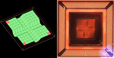
Figure 7. A cross-like pattern is created on the DM surface by applying the voltages necessary for maximum deflection of the 44 actuators that comprise the middle two rows and middle two columns of the array. The frame on the left shows a screen shot of the AO kit software depicting the DM surface, whereas the frame on the right, which was obtained through quasi-dark field illumination, shows the actual DM surface when programmed to these settings. Note that the white light source used for illumination is visible in the lower right-hand corner of the photograph.
Figure 7 (left frame) shows a screen shot of a cross formed on the 12 x 12 actuator array of the DM included with the adaptive optics kit. To create this screen shot, the voltages applied to the middle two rows and middle two columns of actuators were set to cause full deflection of the mirror membrane. In addition to the software screen shot depicting the DM surface, quasi-dark field illumination was used to obtain a photograph of the actual DM surface when programmed to these settings (see Fig. 7, right frame)
The Control Software:
In an adaptive optics setup, the control software is the vital link between the wavefront sensor and the deformable mirror. It converts the wavefront sensor’s electrical signals, which are proportional to the slope of the wavefront, into compensating voltage commands that are sent to each actuator of the DM. The closed-loop bandwidth of the adaptive optics system is directly related to the speed and accuracy with which this computation is done, but in general, these calculations must occur on a shorter time scale than the aberration fluctuations.
In essence, the control software uses the spot field deviations to reconstructs the phase of the beam (in this case, using Zernike polynomials) and then sends conjugate commands to the DM. A least-squares fitting routine is applied to the calculated wavefront phase in order to determine the effective Zernike polynomial data outputted for the end user. Although not the only form possible, Zernike polynomials provide a unique and convenient way to describe the phase of a beam. These polynomials form an orthogonal basis set over a unit circle with different terms representing the amount of focus, tilt, astigmatism, comma, et cetera; the polynomials are normalized so that the maximum of each term (except the piston term) is +1, the minimum is –1, and the average over the surface is always zero. Furthermore, no two aberrations ever add up to a third, thereby leaving no doubt about the type of aberration that is present.
| Damage Threshold Specificationsa | ||
|---|---|---|
| Item # Suffix | Laser Type | Damage Threshold |
| -F01 | CWb | 1 W/cm (250 nm - 450 nm) |
| Pulsed | 0.2 J/cm2 (355 nm, 10 ns, 10 Hz, Ø0.38 mm) | |
| -P01 | CWb | 4 W/cm (450 nm - 2 µm) |
| Pulsed | 1 J/cm2 (1064 nm, 10 ns, 10 Hz, Ø10 mm) | |
Damage Threshold Data for our Piezoelectric Deformable Mirrors
The specifications to the right apply to Thorlabs' Piezoelectric Deformable Mirrors. Please note that the damage threshold is affected by the thin, flexible design of the mirrors and is lower than the damage threshold for our other mirrors that use Thorlabs' standard metallic coatings.
Laser Induced Damage Threshold Tutorial
The following is a general overview of how laser induced damage thresholds are measured and how the values may be utilized in determining the appropriateness of an optic for a given application. When choosing optics, it is important to understand the Laser Induced Damage Threshold (LIDT) of the optics being used. The LIDT for an optic greatly depends on the type of laser you are using. Continuous wave (CW) lasers typically cause damage from thermal effects (absorption either in the coating or in the substrate). Pulsed lasers, on the other hand, often strip electrons from the lattice structure of an optic before causing thermal damage. Note that the guideline presented here assumes room temperature operation and optics in new condition (i.e., within scratch-dig spec, surface free of contamination, etc.). Because dust or other particles on the surface of an optic can cause damage at lower thresholds, we recommend keeping surfaces clean and free of debris. For more information on cleaning optics, please see our Optics Cleaning tutorial.
Testing Method
Thorlabs' LIDT testing is done in compliance with ISO/DIS 11254 and ISO 21254 specifications.
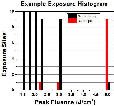
First, a low-power/energy beam is directed to the optic under test. The optic is exposed in 10 locations to this laser beam for 30 seconds (CW) or for a number of pulses (pulse repetition frequency specified). After exposure, the optic is examined by a microscope (~100X magnification) for any visible damage. The number of locations that are damaged at a particular power/energy level is recorded. Next, the power/energy is either increased or decreased and the optic is exposed at 10 new locations. This process is repeated until damage is observed. The damage threshold is then assigned to be the highest power/energy that the optic can withstand without causing damage. A histogram such as that below represents the testing of one BB1-E02 mirror.
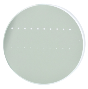
The photograph above is a protected aluminum-coated mirror after LIDT testing. In this particular test, it handled 0.43 J/cm2 (1064 nm, 10 ns pulse, 10 Hz, Ø1.000 mm) before damage.
| Example Test Data | |||
|---|---|---|---|
| Fluence | # of Tested Locations | Locations with Damage | Locations Without Damage |
| 1.50 J/cm2 | 10 | 0 | 10 |
| 1.75 J/cm2 | 10 | 0 | 10 |
| 2.00 J/cm2 | 10 | 0 | 10 |
| 2.25 J/cm2 | 10 | 1 | 9 |
| 3.00 J/cm2 | 10 | 1 | 9 |
| 5.00 J/cm2 | 10 | 9 | 1 |
According to the test, the damage threshold of the mirror was 2.00 J/cm2 (532 nm, 10 ns pulse, 10 Hz, Ø0.803 mm). Please keep in mind that these tests are performed on clean optics, as dirt and contamination can significantly lower the damage threshold of a component. While the test results are only representative of one coating run, Thorlabs specifies damage threshold values that account for coating variances.
Continuous Wave and Long-Pulse Lasers
When an optic is damaged by a continuous wave (CW) laser, it is usually due to the melting of the surface as a result of absorbing the laser's energy or damage to the optical coating (antireflection) [1]. Pulsed lasers with pulse lengths longer than 1 µs can be treated as CW lasers for LIDT discussions.
When pulse lengths are between 1 ns and 1 µs, laser-induced damage can occur either because of absorption or a dielectric breakdown (therefore, a user must check both CW and pulsed LIDT). Absorption is either due to an intrinsic property of the optic or due to surface irregularities; thus LIDT values are only valid for optics meeting or exceeding the surface quality specifications given by a manufacturer. While many optics can handle high power CW lasers, cemented (e.g., achromatic doublets) or highly absorptive (e.g., ND filters) optics tend to have lower CW damage thresholds. These lower thresholds are due to absorption or scattering in the cement or metal coating.

LIDT in linear power density vs. pulse length and spot size. For long pulses to CW, linear power density becomes a constant with spot size. This graph was obtained from [1].
Pulsed lasers with high pulse repetition frequencies (PRF) may behave similarly to CW beams. Unfortunately, this is highly dependent on factors such as absorption and thermal diffusivity, so there is no reliable method for determining when a high PRF laser will damage an optic due to thermal effects. For beams with a high PRF both the average and peak powers must be compared to the equivalent CW power. Additionally, for highly transparent materials, there is little to no drop in the LIDT with increasing PRF.
In order to use the specified CW damage threshold of an optic, it is necessary to know the following:
- Wavelength of your laser
- Beam diameter of your beam (1/e2)
- Approximate intensity profile of your beam (e.g., Gaussian)
- Linear power density of your beam (total power divided by 1/e2 beam diameter)
Thorlabs expresses LIDT for CW lasers as a linear power density measured in W/cm. In this regime, the LIDT given as a linear power density can be applied to any beam diameter; one does not need to compute an adjusted LIDT to adjust for changes in spot size, as demonstrated by the graph to the right. Average linear power density can be calculated using the equation below.

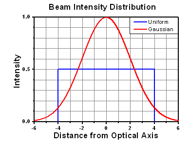
The calculation above assumes a uniform beam intensity profile. You must now consider hotspots in the beam or other non-uniform intensity profiles and roughly calculate a maximum power density. For reference, a Gaussian beam typically has a maximum power density that is twice that of the uniform beam (see lower right).
Now compare the maximum power density to that which is specified as the LIDT for the optic. If the optic was tested at a wavelength other than your operating wavelength, the damage threshold must be scaled appropriately. A good rule of thumb is that the damage threshold has a linear relationship with wavelength such that as you move to shorter wavelengths, the damage threshold decreases (i.e., a LIDT of 10 W/cm at 1310 nm scales to 5 W/cm at 655 nm):

While this rule of thumb provides a general trend, it is not a quantitative analysis of LIDT vs wavelength. In CW applications, for instance, damage scales more strongly with absorption in the coating and substrate, which does not necessarily scale well with wavelength. While the above procedure provides a good rule of thumb for LIDT values, please contact Tech Support if your wavelength is different from the specified LIDT wavelength. If your power density is less than the adjusted LIDT of the optic, then the optic should work for your application.
Please note that we have a buffer built in between the specified damage thresholds online and the tests which we have done, which accommodates variation between batches. Upon request, we can provide individual test information and a testing certificate. The damage analysis will be carried out on a similar optic (customer's optic will not be damaged). Testing may result in additional costs or lead times. Contact Tech Support for more information.
Pulsed Lasers
As previously stated, pulsed lasers typically induce a different type of damage to the optic than CW lasers. Pulsed lasers often do not heat the optic enough to damage it; instead, pulsed lasers produce strong electric fields capable of inducing dielectric breakdown in the material. Unfortunately, it can be very difficult to compare the LIDT specification of an optic to your laser. There are multiple regimes in which a pulsed laser can damage an optic and this is based on the laser's pulse length. The highlighted columns in the table below outline the relevant pulse lengths for our specified LIDT values.
Pulses shorter than 10-9 s cannot be compared to our specified LIDT values with much reliability. In this ultra-short-pulse regime various mechanics, such as multiphoton-avalanche ionization, take over as the predominate damage mechanism [2]. In contrast, pulses between 10-7 s and 10-4 s may cause damage to an optic either because of dielectric breakdown or thermal effects. This means that both CW and pulsed damage thresholds must be compared to the laser beam to determine whether the optic is suitable for your application.
| Pulse Duration | t < 10-9 s | 10-9 < t < 10-7 s | 10-7 < t < 10-4 s | t > 10-4 s |
|---|---|---|---|---|
| Damage Mechanism | Avalanche Ionization | Dielectric Breakdown | Dielectric Breakdown or Thermal | Thermal |
| Relevant Damage Specification | No Comparison (See Above) | Pulsed | Pulsed and CW | CW |
When comparing an LIDT specified for a pulsed laser to your laser, it is essential to know the following:
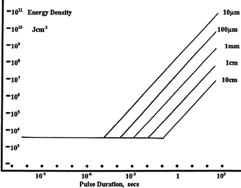
LIDT in energy density vs. pulse length and spot size. For short pulses, energy density becomes a constant with spot size. This graph was obtained from [1].
- Wavelength of your laser
- Energy density of your beam (total energy divided by 1/e2 area)
- Pulse length of your laser
- Pulse repetition frequency (prf) of your laser
- Beam diameter of your laser (1/e2 )
- Approximate intensity profile of your beam (e.g., Gaussian)
The energy density of your beam should be calculated in terms of J/cm2. The graph to the right shows why expressing the LIDT as an energy density provides the best metric for short pulse sources. In this regime, the LIDT given as an energy density can be applied to any beam diameter; one does not need to compute an adjusted LIDT to adjust for changes in spot size. This calculation assumes a uniform beam intensity profile. You must now adjust this energy density to account for hotspots or other nonuniform intensity profiles and roughly calculate a maximum energy density. For reference a Gaussian beam typically has a maximum energy density that is twice that of the 1/e2 beam.
Now compare the maximum energy density to that which is specified as the LIDT for the optic. If the optic was tested at a wavelength other than your operating wavelength, the damage threshold must be scaled appropriately [3]. A good rule of thumb is that the damage threshold has an inverse square root relationship with wavelength such that as you move to shorter wavelengths, the damage threshold decreases (i.e., a LIDT of 1 J/cm2 at 1064 nm scales to 0.7 J/cm2 at 532 nm):

You now have a wavelength-adjusted energy density, which you will use in the following step.
Beam diameter is also important to know when comparing damage thresholds. While the LIDT, when expressed in units of J/cm², scales independently of spot size; large beam sizes are more likely to illuminate a larger number of defects which can lead to greater variances in the LIDT [4]. For data presented here, a <1 mm beam size was used to measure the LIDT. For beams sizes greater than 5 mm, the LIDT (J/cm2) will not scale independently of beam diameter due to the larger size beam exposing more defects.
The pulse length must now be compensated for. The longer the pulse duration, the more energy the optic can handle. For pulse widths between 1 - 100 ns, an approximation is as follows:

Use this formula to calculate the Adjusted LIDT for an optic based on your pulse length. If your maximum energy density is less than this adjusted LIDT maximum energy density, then the optic should be suitable for your application. Keep in mind that this calculation is only used for pulses between 10-9 s and 10-7 s. For pulses between 10-7 s and 10-4 s, the CW LIDT must also be checked before deeming the optic appropriate for your application.
Please note that we have a buffer built in between the specified damage thresholds online and the tests which we have done, which accommodates variation between batches. Upon request, we can provide individual test information and a testing certificate. Contact Tech Support for more information.
[1] R. M. Wood, Optics and Laser Tech. 29, 517 (1998).
[2] Roger M. Wood, Laser-Induced Damage of Optical Materials (Institute of Physics Publishing, Philadelphia, PA, 2003).
[3] C. W. Carr et al., Phys. Rev. Lett. 91, 127402 (2003).
[4] N. Bloembergen, Appl. Opt. 12, 661 (1973).
In order to illustrate the process of determining whether a given laser system will damage an optic, a number of example calculations of laser induced damage threshold are given below. For assistance with performing similar calculations, we provide a spreadsheet calculator that can be downloaded by clicking the button to the right. To use the calculator, enter the specified LIDT value of the optic under consideration and the relevant parameters of your laser system in the green boxes. The spreadsheet will then calculate a linear power density for CW and pulsed systems, as well as an energy density value for pulsed systems. These values are used to calculate adjusted, scaled LIDT values for the optics based on accepted scaling laws. This calculator assumes a Gaussian beam profile, so a correction factor must be introduced for other beam shapes (uniform, etc.). The LIDT scaling laws are determined from empirical relationships; their accuracy is not guaranteed. Remember that absorption by optics or coatings can significantly reduce LIDT in some spectral regions. These LIDT values are not valid for ultrashort pulses less than one nanosecond in duration.

A Gaussian beam profile has about twice the maximum intensity of a uniform beam profile.
CW Laser Example
Suppose that a CW laser system at 1319 nm produces a 0.5 W Gaussian beam that has a 1/e2 diameter of 10 mm. A naive calculation of the average linear power density of this beam would yield a value of 0.5 W/cm, given by the total power divided by the beam diameter:

However, the maximum power density of a Gaussian beam is about twice the maximum power density of a uniform beam, as shown in the graph to the right. Therefore, a more accurate determination of the maximum linear power density of the system is 1 W/cm.
An AC127-030-C achromatic doublet lens has a specified CW LIDT of 350 W/cm, as tested at 1550 nm. CW damage threshold values typically scale directly with the wavelength of the laser source, so this yields an adjusted LIDT value:

The adjusted LIDT value of 350 W/cm x (1319 nm / 1550 nm) = 298 W/cm is significantly higher than the calculated maximum linear power density of the laser system, so it would be safe to use this doublet lens for this application.
Pulsed Nanosecond Laser Example: Scaling for Different Pulse Durations
Suppose that a pulsed Nd:YAG laser system is frequency tripled to produce a 10 Hz output, consisting of 2 ns output pulses at 355 nm, each with 1 J of energy, in a Gaussian beam with a 1.9 cm beam diameter (1/e2). The average energy density of each pulse is found by dividing the pulse energy by the beam area:

As described above, the maximum energy density of a Gaussian beam is about twice the average energy density. So, the maximum energy density of this beam is ~0.7 J/cm2.
The energy density of the beam can be compared to the LIDT values of 1 J/cm2 and 3.5 J/cm2 for a BB1-E01 broadband dielectric mirror and an NB1-K08 Nd:YAG laser line mirror, respectively. Both of these LIDT values, while measured at 355 nm, were determined with a 10 ns pulsed laser at 10 Hz. Therefore, an adjustment must be applied for the shorter pulse duration of the system under consideration. As described on the previous tab, LIDT values in the nanosecond pulse regime scale with the square root of the laser pulse duration:

This adjustment factor results in LIDT values of 0.45 J/cm2 for the BB1-E01 broadband mirror and 1.6 J/cm2 for the Nd:YAG laser line mirror, which are to be compared with the 0.7 J/cm2 maximum energy density of the beam. While the broadband mirror would likely be damaged by the laser, the more specialized laser line mirror is appropriate for use with this system.
Pulsed Nanosecond Laser Example: Scaling for Different Wavelengths
Suppose that a pulsed laser system emits 10 ns pulses at 2.5 Hz, each with 100 mJ of energy at 1064 nm in a 16 mm diameter beam (1/e2) that must be attenuated with a neutral density filter. For a Gaussian output, these specifications result in a maximum energy density of 0.1 J/cm2. The damage threshold of an NDUV10A Ø25 mm, OD 1.0, reflective neutral density filter is 0.05 J/cm2 for 10 ns pulses at 355 nm, while the damage threshold of the similar NE10A absorptive filter is 10 J/cm2 for 10 ns pulses at 532 nm. As described on the previous tab, the LIDT value of an optic scales with the square root of the wavelength in the nanosecond pulse regime:

This scaling gives adjusted LIDT values of 0.08 J/cm2 for the reflective filter and 14 J/cm2 for the absorptive filter. In this case, the absorptive filter is the best choice in order to avoid optical damage.
Pulsed Microsecond Laser Example
Consider a laser system that produces 1 µs pulses, each containing 150 µJ of energy at a repetition rate of 50 kHz, resulting in a relatively high duty cycle of 5%. This system falls somewhere between the regimes of CW and pulsed laser induced damage, and could potentially damage an optic by mechanisms associated with either regime. As a result, both CW and pulsed LIDT values must be compared to the properties of the laser system to ensure safe operation.
If this relatively long-pulse laser emits a Gaussian 12.7 mm diameter beam (1/e2) at 980 nm, then the resulting output has a linear power density of 5.9 W/cm and an energy density of 1.2 x 10⁻⁴ J/cm2 per pulse. This can be compared to the LIDT values for a WPQ10E-980 polymer zero-order quarter-wave plate, which are 5 W/cm for CW radiation at 810 nm and 5 J/cm2 for a 10 ns pulse at 810 nm. As before, the CW LIDT of the optic scales linearly with the laser wavelength, resulting in an adjusted CW value of 6 W/cm at 980 nm. On the other hand, the pulsed LIDT scales with the square root of the laser wavelength and the square root of the pulse duration, resulting in an adjusted value of 55 J/cm2 for a 1 µs pulse at 980 nm. The pulsed LIDT of the optic is significantly greater than the energy density of the laser pulse, so individual pulses will not damage the wave plate. However, the large average linear power density of the laser system may cause thermal damage to the optic, much like a high-power CW beam.
| Posted Comments: | |
Axin Fan
(posted 2024-03-18 17:28:26.743) Hi, I am using DMH40/M-P01. Can you provide a Python script to control it? Thank you very much. fmortaheb
(posted 2024-03-19 08:59:03.0) Thank you very much for contacting us. The Python scripts for the deformable mirrors can be found here: https://github.com/Thorlabs/Light_Control_and_Manipulation_Examples/tree/main/Python/DMP40%20DMH40%20Deformable%20Mirrors Guillaume Dovillaire
(posted 2023-12-21 12:55:16.267) Hi,
Do you provide a linux distribution of your DMP40 ?
Thanks,
Guillaume dpossin
(posted 2024-01-02 05:39:27.0) Dear Guillaume,
Thank you for your feedback. I´ll reach out to you in order to provide further assistance. user
(posted 2023-10-20 16:34:32.97) Please provide support for MATLAB - You have had many requests regarding this. I see the comments where you give instructions to use loadlibrary and calllib, but you dont, for example, mention that you need to load multiple DLLs. It would be greatly appreciated if you could provide a sample script that you verified works at least on your end. GBoedecker
(posted 2023-10-23 11:24:56.0) Thank you for your feedback! I will contact you directly to provide assistance with Matlab. Miltcho Danailov
(posted 2022-12-20 16:31:54.077) Question concerning the mirror protective silver coating:
- any data on LIDT with femtosecond pulses?
- is the coating same as in your standard protected silver mirrors so we could test?
- is it possible to replace the mirror only, e.g. in case of surface damage? wskopalik
(posted 2022-12-21 07:45:10.0) Thank you for your feedback!
Unfortunately, we do not have any LIDT data for fs lasers. The coating itself is similar to the standard mirrors, but due to the thinner substrate the performance regarding LIDT will be different, i.e. the damage threshold values are lower than on the standard mirrors.
The deformable mirror is permanently attached to the actuators so in case of a damage the whole mirror unit needs to be exchanged.
I will contact you directly so we can talk about your application in more detail. Daozheng Gong
(posted 2022-10-25 12:32:27.99) Hello,
Our lab is currently using the DMH40-P01, and we found one thing that confuses us about the software. When changing the Zernike coefficient for defocus (Z5), all segments are displaying the same color change in the schematics, indicating all the segments of the deformable mirror is having the same displacement. In other words, the deformable mirror is actually changing the piston, instead of defocusing. Would it be possible for you to check if the functions for Zernike polynomial set in the software are correct?
Best,
Daozheng wskopalik
(posted 2022-11-07 05:39:08.0) Thank you very much for your feedback!
The colors in the “Mirror Control” display in the software correspond only to the applied voltage to each actuator and not to the deformation of the mirror surface. An applied voltage will lead to an expansion or contraction of the actuator which in turn deforms the mirror surface to a concave or convex shape. I.e. you could derive the surface deformation from the voltage values in the display, but it is not a direct representation.
For the spherical deformation of the defocus coefficient Z5, all the mirror segments need to be deformed in the same concave or convex way. That is why the same voltage is applied to all segments and why the color is the same for all segments in the display.
I will contact you directly for further discussion. Edison Gerena
(posted 2022-07-25 12:22:29.22) Hi, we would like to run the DM under linux environment. The DMP40-P01 has a linux software development tool ? bwuensch
(posted 2022-08-01 06:27:36.0) Dear Edison Gerena, Thank you for your feedback. I will contact you directly to provide further assistance. user
(posted 2022-03-01 21:21:19.283) Hi,
Can you share with me a Matlab testing code for DMP40-P01? Thank you.
I also have an error code saying Call Library Function Node 'TLDFM_fet_voltages': Library not found with the Labview driver you provided with the installation package. I would appreciate the help to solve the error. wskopalik
(posted 2022-03-03 10:53:27.0) Thank you very much for your feedback!
Unfortunately, we do not have an example code for MATLAB for these deformable mirrors. You can e.g. use the "loadlibrary" command in MATLAB to load the driver files we provide into MATLAB. After the driver files have been loaded, the command "calllib" can be used to access the functions implemented in these files, i.e. to control the deformable mirror.
I will contact you directly to provide further assistance about this and about the error message in LabView. user
(posted 2022-01-21 11:40:42.75) Hi-
Is there a labview vi for getting the feedback signal? I don't see anything in the library. For example, I want to implement closed loop feedback w/ PDA10 by reading the signal from the mirror and feeding it into an optimization code. Is this possible to do from the mirror?
Thanks :) wskopalik
(posted 2022-01-24 09:26:05.0) Thank you very much for your feedback!
You can use one of these VIs: “TLDFM Get Feedback Current.vi” and “TLDFM Get Feedback Voltage.vi” will return the current or the voltage applied to the analog feedback input. “TLDFM Get Feedback.vi” will return both.
The PDA10 detectors have a voltage output signal. So “TLDFM Get Feedback Voltage.vi” will probably be the most suitable VI in your application.
Please note that the analog feedback input is designed for voltages between 0 – 2.5 V. So you would need to make sure that this voltage level is no exceeded by the PDA10 detector.
I will also contact you directly to provide further assistance. user
(posted 2021-09-13 16:30:02.99) Hello. I have bought DMP40-P01 for abberation correction. Could you please provide matlab diver for this hardware ?
I also notice this DM supports Zernike term 4 to Zernike term 15. Could you please provide mathematic(al) expressions for those term? thanks a lot! wskopalik
(posted 2021-09-17 05:23:27.0) Thank you very much for your feedback!
Unfortunately, we do not have an example code for MATLAB for these deformable mirrors. You can e.g. use the "loadlibrary" command in MATLAB to load the driver files we provide into MATLAB. After the driver files have been loaded, the command "calllib" can be used to access the functions implemented in these files, i.e. to control the deformable mirror.
I will contact you directly to provide further information about this and about the mathematical expressions. Jungbin Lee
(posted 2021-03-24 22:00:09.103) Hello. I have DMH40/M-P01 and WFS40-7AR. And until now, I used the basic software to do closed loop control and this has been successful. Now, I want to do closed loop control using labview, but I am curious if the labview example code provides a closed loop control function or not. wskopalik
(posted 2021-03-26 07:12:12.0) Thank you very much for your feedback!
The LabVIEW example codes which are provided in the software packages of the deformable mirror and of the wavefront sensor only show the use of each device individually. They do not include a closed loop control.
It is however possible to implement a closed loop in LabVIEW using the provided VIs. You would at first measure the wavefront deformation on the wavefront sensor and then use this data to create a corresponding pattern on the deformable mirror. There are a couple of VIs which can be used for that.
I will contact you directly to provide further assistance. user
(posted 2021-01-21 19:04:37.58) Hello, I am considering the purchase of one of the deformable mirros and wavefront sensor systems for use in a femtosecond laser system. Do you have any information on the damage threshold for femtosecond and picosecond laser pulses.
thanks MKiess
(posted 2021-01-25 09:04:35.0) Thank you very much for your feedback. Unfortunately, we do not have test data regarding the damage threshold for femtosecond or picosecond lasers, for our piezoelectric deformable mirrosrs. But, the general specification for silver coated mirrors, adapted to the thinner substrate and coating thickness, which is used at the DMH would be the damage threshold value of 0.1J/cm² (800nm, 99fs, pulsed, 1 kHz, dia 0.167mm). Jungbin Lee
(posted 2020-10-20 04:40:08.56) Hello, I bought DMH40/M-P01. I'd like to ask for a Matlab example for this deformable mirror. And can i make a closed loop control with wavefront sensor (I also bought WFS40-7AR/M) in matlab? wskopalik
(posted 2020-10-21 11:03:49.0) Thank you very much for your feedback!
Unfortunately, we don't have an example code for MATLAB for these deformable mirrors. You can e.g. use the "loadlibrary" command in MATLAB to load the driver files we provide into MATLAB. After the driver files have been loaded, the command "calllib" can be used to access the functions implemented in these files, i.e. to control the deformable mirror. It is also possible to program a closed loop with these functions.
I will contact you directly to provide further information about how this works in detail. user
(posted 2020-10-14 07:49:12.917) Hello. We have the AOK7/M-P01 and the AOKit software on the PC can't detect the DMP40/M-P01. When we connect the usb cable and the DC plug on the power supply shipped with the DM, We can see a green light for 5 seconds on the DM wich turn to red immediatiadtly. So the AO Kit application detect the wavefront sensor but not the DM. However, we had download previously the correct drivers on the PC for the DM. Thank you. wskopalik
(posted 2020-10-19 11:13:55.0) Thank you very much for your feedback!
I have contacted you directly so we can find a solution for this issue with the AOKit software. Richard KK
(posted 2020-09-18 17:57:58.497) Hello, I'm using the C++ library in my application. After calling TLDFMX_measure_system_parameters(with measured Zernike amplitudes all equals to 0, and looped until remaining steps is 0) at first, I called TLDFMX_convert_measured_zernike_amplitudes, which returned all the device Zernike amplitudes with +/-inf value(which should be within +/-1, according to the manual). Could you make it clear what is the correct way to use those two functions? Actually I just want to use the mirror to generate certain wavefront patterns with calculated Zernike amplitudes. What is the easiest way to do that? MKiess
(posted 2020-09-23 06:33:13.0) Dear Richard, thank you for contacting Thorlabs. I have contacted you directly to discuss your program with you in detail. Jungbin Lee
(posted 2020-08-26 00:43:49.527) Hello, I'd like to ask for some questions about DMH40/M-P01 model. First, the Surface Flatness (RMS) is 200 nm, but this is about half the wavelength of light, isn't it quite high?. Second, how accurately can this model control hte defocus?. For example, the mems deformable mirror's resolution is 14bit. But this piezoelectric model doesn't provide the information. Third, can i make defocus without wavefront sensor? dpossin
(posted 2020-08-27 04:45:50.0) Dear Lee,
Thank you for your feedback. Please see the answers to your questions below:
1). You need to see this value in relation to the quite large available amplitude of +/- 6.5 µm peak to valley. The mirror uses a very thin 120µm glassubstrate which can not be produced within the same surface quality like thicker optics. Additionally there are abberations due to the bonding onto the very thin piezoelectric plate. The RMS value we spec just gives the surface quality you get, when the 40 segments of the mirror are driven with an average voltage of 100V. Via active feedback loop, the mirror can compensate its own abberation such that RMS values of 1nm can be reached. Therefore voltage patterns of about 20% of the available range (0-200V) are needed. Taking this into account, you still have 80% of the full stroke left for your application.
2). Well the RMS value we spec refers to the defocus therm, so the accuracy in the active control loop can also reach 1nm.
3). I will discuss this question with you directly. Boyu Gu
(posted 2019-04-08 13:32:52.55) Hello. I'm creating my application using C++. I tried to use the function "TLDFMX_convert_measured_zernike_amplitudes", but it always return an error "Measured system parameters are invalid".
could you please give me an instruction about this function. wskopalik
(posted 2019-04-09 10:23:29.0) This is a response from Wolfgang at Thorlabs. Thank you very much for your feedback!
As a precondition to run the function "TLDFMX_convert_measured_zernike_amplitudes()" you would first need to run the function "TLDFMX_measure_system_parameters()" successfully. If this function is run before, "TLDFMX_convert_measured_zernike_amplitudes()" will work properly. Otherwise the error message “Measured system parameters are invalid” will be returned.
Further information about the driver functions can be found in the help files and I will also contact you directly to provide further assistance. pablo.meza
(posted 2018-09-30 08:14:51.987) Good day. Can you share a procedure to load up the driver for the DM into Matlab? Thank you in advance wskopalik
(posted 2018-10-04 10:18:01.0) This is a response from Wolfgang at Thorlabs. Thank you very much for your feedback.
You can use the "loadlibrary" command in MATLAB to load the driver files we provide into MATLAB. After the driver files have been loaded, the command "calllib" can be used to access the functions implemented in these files, i.e. to control the deformable mirror.
I will contact you directly to provide further information about how this works in detail. zhuhai
(posted 2018-08-30 00:29:40.313) Good day. I'd like to ask for a Matlab example for this deformable mirror. Thanks. wskopalik
(posted 2018-09-06 04:50:00.0) This is a response from Wolfgang at Thorlabs. Thank you very much for your feedback.
In MATLAB the "loadlibrary" command can be used to load the driver files we provide into MATLAB. After the driver files have been loaded, the command "calllib" can be used to access the functions implemented in these files, i.e. to control the deformable mirror.
I will contact you directly to provide further information about how this works in detail. user
(posted 2018-06-05 12:07:21.823) swick: You do ship a 64 bit library which needs the 64 bit runtime. Nowhere in the documentation it is mentioned that I need to install something else. Since there is no error message, please include the 64-runtime or mention it VERY VISIBLE in the docs. I lost two days of work for that. mvonsivers
(posted 2018-06-08 09:41:09.0) This is a response from Moritz at Thorlabs. Thank you for your feedback. I will forward your suggestion to our software development. user
(posted 2018-04-19 14:45:25.57) The installer of the software is missing the 64 bit NI CVI Runtime. Therefore using the 64 bit does not work. swick
(posted 2018-05-14 03:16:16.0) This is a response from Sebastian at Thorlabs. Thank you for the inquiry.
The NI CVI Runtime is required for the programmer examples, which are made for 32-bit. Therefore only the 32-bit NI CVI runtime is included to the installer. muw445
(posted 2017-10-19 11:37:05.777) We plan to use the deformable mirrors in the field where it is hard to take laptops along. So I'd like to know if it's possible that we develop our own control softwares and drivers, for example, with an embedded system? Windows is not an option for us. wskopalik
(posted 2017-10-20 10:26:21.0) This is a response from Wolfgang at Thorlabs. Thank you very much for your inquiry.
The software and the driver files for these deformable mirrors are only available for Windows systems. We don't have any solution for Linux at the moment.
I will contact you directly to discuss your application in detail. akiyama
(posted 2016-10-21 16:53:16.13) Does DMP40-P01 have a linux software development tool ? We would like to run the DM under linux environment. swick
(posted 2016-10-21 05:19:45.0) This is a response from Sebastian at Thorlabs. Thank you for the inquiry.
Our software and drivers for DMP40-P01 are only compatible with Windows based operating systems. clement.fallet
(posted 2015-08-21 15:08:09.09) Is it possible to use this DMP40 at 45° incidence? In addition to provide wavefront correction, I also want it to reflect at 90° my input beam.
What is the best way to control it in this case?
I see that the provided software operates on the Zernike polynoms basis but with the assumption that this is normal incidence and thus have a circular pupil.
Is there a way to modify it to take into account an elliptical pupil?
Thank you for your help.
Dr. Clement Fallet shallwig
(posted 2015-08-24 09:38:28.0) This is a response from Stefan at Thorlabs. Thank you very much for your inquiry. It is not recommended to use the piezo electric deformable mirror at 45° angle of incidence. The design of our mirrors is circular and the software also calculates on basis of a circular beam hitting the mirror . As you said at 45° angle of incidence you would get an elliptical beam shape and at the moment we cannot offer a Piezo disk with this shape to compensate that. The number of controllable segments within the pupil diameter is with 24 too little to compensate such elliptical beam shape through the software. By a higher number of segments and just using the segments corresponding to the beam shape this could be achieved more accurately.
The most accurate way to deal with that problem would be to use a beam splitter as used in the reference setup described in the manual from page 59 http://www.thorlabs.de/thorcat/MTN/DMP40_M-P01-Manual.pdf
This way the incident beam hits the mirror at 90° as it is supposed to but the beam gets reflected at 90°. Disadvantage of this assembly is the loss of light. Alternatively you could set the deformable mirror for example at 80° though you would still have an elliptical beam but not as strong as at 45° and with a second mirror you could get the 90° redirection you are looking for. I will contact you directly to discuss your application in detail. voronov.alexander
(posted 2015-04-06 18:41:41.78) Is it possible to order DMP40/M-P01 with protected aluminium coating in order to use with 355nm laser(<30mW)? shallwig
(posted 2015-04-10 02:34:09.0) This is a response from Stefan at Thorlabs. Thank you very much for your inquiry. We are checking if it is possible to offer a special version with aluminum coating for UV applications. I will contact you directly to discuss your further requirements. yoshihiro_kazama
(posted 2015-01-22 19:54:12.653) Dear Thorlabs. Inc
Im engineer who bought deformable mirro DMP40,
and have a question about "Thorlabs DFM Visa Instrument Driver".
To control DMP, I use
1.(first)
TLDFM_get_segment_voltage
TLDFM_set_segment_voltage
2.(second)
TLDFM_get_segment_voltages
TLDFM_set_segment_voltages
3.(third)
TLDFM_get_voltages
TLDFM_set_voltages
In first function, I can set voltage to each segment one by one. And I got different value between Setpoint and Actual.
I think it comes from Hysterisis compensation.
In second & third function, I can set voltage at once to all segments. And I go "same" value between Setpoint and Actual.
I get confused about this difference, because I havent get & set hysteresis_parameters in sample program.
Im looking forward to your reply.
Best regard
Yoshihiro Kazama shallwig
(posted 2015-01-23 03:07:14.0) This is a response from Stefan at Thorlabs. Thank you very much for your inquiry. We will contact you directly to troubleshoot this problem in detail. pedro.escarate
(posted 2015-01-07 07:54:18.823) I would like a detail of the components of the application idea presented for DMP40-P01 shallwig
(posted 2015-01-07 08:21:42.0) This is a response from Stefan at Thorlabs. Thank you very much for your inquiry. We have listed the parts used in the application idea in the manual on page 70-71:
http://www.thorlabs.de/thorcat/MTN/DMP40_M-P01-Manual.pdf
I will contact you directly to check if you need further information. |
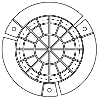
Click for Details
The circular keystone actuator array used by the DMP40 piezoelectric deformable mirrors.
Considerations
Ideally, the deformable mirror needs to assume a surface shape that is complementary to, but half the amplitude of, the aberration profile in order to compensate for the aberrations and yield a flat wavefront. However, the actual range of wavefronts that can be corrected by a particular deformable mirror is limited by several factors:
- Actuator stroke is another term for the dynamic range (i.e., the maximum displacement) of the deformable mirror actuators and is typically measured in microns. Inadequate actuator stroke leads to poor performance by limiting aberration amplitudes that may be compensated, preventing the convergence of the control loop.
- The number of actuators limits the degrees of freedom of the wavefront control system, and therefore the complexity of the wavefront that may be corrected.
- The speed of the deformable mirror is important if you are trying to correct for rapidly changing wavefronts. For mirrors that exhibit hysteresis (i.e., piezoelectric deformable mirrors), the control software will need to calculate the correct voltage changes to produce the desired mirror displacement, which can lower the mirror speed.
- Optical power handling will also vary depending on the mirror coating and actuator design. For our mirrors, the piezoelectric deformable mirrors have significantly higher power handling than the MEMS systems [up to 1 J/cm² (1064 nm, 10 ns, 10 Hz, Ø10 mm) for the protected silver coated versions]. They can also be custom coated to operate inside laser cavities (contact Tech Support for details).
- Hysteresis in piezoelectric deformable mirrors means that the displacement of a mirror segment at a given voltage is different if that voltage is approached from a higher voltage compared to a lower voltage. Our piezoelectric deformable mirrors offer hysteresis compensation when used with Thorlabs' control software, while the MEMS-based deformable mirrors are inherently hysteresis-free. The hysteresis compensation for the piezoelectric deformable mirrors can be turned off when operating the mirror with open-loop control, which can increase the speed.
The first four considerations are physical limitations of the deformable mirror itself, whereas hysteresis may be a limitation of the control software and/or a physical limitation of the mirror itself. Additionally, the wavelength range of the deformable mirror coating and any protective windows installed in the mirror head must be appropriate for the application wavelength.
Comparison
Thorlabs' piezoelectric deformable mirrors provide a larger stroke, and therefore are able to correct for larger wavefront deviations, than our MEMS-based deformable mirrors. However, they contain a lower density of actuators over the active area of the mirror than the MEMS-based Multi DMs below, which means they cannot correct wavefront deviations on as fine of a spatial scale as the MEMS-based DMs.
To correct for both large amplitude and small spatial scale wavefront distortions, consider using a piezoelectric and MEMS-based deformable mirror in tandem, typically referred to in the literature as a woofer-tweeter configuration. The piezoelectric deformable mirror can correct for the tip, tilt, and lower order (lower spatial frequency) wavefront distortions, while the MEMS-based device compensates for higher order (higher spatial frequency) wavefront distortions. In nature, lower order wavefront distortions typically have larger magnitudes than do higher order wavefront distortions. Therefore, the combination of our lower actuator count, larger displacement, piezo-based DM and the higher actuator count, smaller displacement, MEMS-based DM is well suited to be used in a woofer-tweeter configuration.
| Deformable Mirror Comparison | |||||||
|---|---|---|---|---|---|---|---|
| Deformable Mirror Type |
MEMS-Based from Boston Micromachines | Piezoelectric | |||||
| Item # | DM140A-35-UP01 | DM140A-35-P01 | DM140A-35-UM01 | DMP40-F01 DMP40/M-F01 |
DMP40-P01 DMP40/M-P01 |
DMH40-F01 DMH40/M-F01 |
DMH40-P01 DMH40/M-P01 |
| Actuator Array | 140 Actuators in a 12 x 12 Array | 40 Piezoceramic Disk Segments in a Circular Keystone Array (Elements 1 - 24 Inside Pupil Diameter, Elements 25 - 40 Outside Pupil Diameter) |
|||||
| Actuator Stroke | 3.5 µm per Actuator | Defocusa: ±6.5 µm Astigmatisma: ±6.8 µm Comaa: ±2.5 µm Trefoila: ±2.4 µm Tetrafoila: ±2.1 µm Secondary Astigmatisma: ±1.1 µm Third Order Spherical Aberrationa: ±1.0 µm |
Defocusa: ±17.6 µm Astigmatisma: ±18.4 µm Comaa: ±6.8 µm Trefoila: ±6.5 µm Tetrafoila: ±5.7 µm Secondary Astigmatisma: ±3.0 µm Third Order Spherical Aberrationa: ±2.7 µm |
||||
| Tip/Tilt | N/A | 3 Spiral Arms for ±2.0 mrad of Tip/Tilt | N/A | ||||
| Pupil Dimensions | 4.4 mm x 4.4 mm | Ø10.0 mm | Ø14.0 mm | ||||
| Mirror Coating (Click for Plot) |
Aluminum | Protected Silver | Gold | UV-Enhanced Aluminum |
Protected Silver | UV-Enhanced Aluminum |
Protected Silver |
| Mirror Wavelength Range |
400 - 1100 nm | 400 - 1100 nm | 600 - 1100 nm | 250 - 450 nm (Ravg > 89%) |
450 nm - 2 µm (Ravg > 97.5%), 2 - 20 µm (Ravg > 96%) |
250 - 450 nm (Ravg > 89%) |
450 nm - 2 µm (Ravg > 97.5%), 2 - 20 µm (Ravg > 96%) |
| Hysteresis | None | 15% Typical, 25% Max | 20% Typical, 25% Max | ||||
| Response Time | <100 µs (~3.5 kHz) Mechanical Response Time (10% - 90%) | 0.5 ms (Full Stroke) Mirror Response Time 5 ms (Full Stroke) Tip/Tilt Response Time |
0.5 ms (Full Stroke) Mirror Response Time | ||||
| Frame Rate (Max) | 8 kHz (34 kHz Bursts) | 4 kHz via USB 2.0 (Over Entire Voltage Range) | |||||

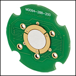
Click to Enlarge
The internal circuit board and mirror of a DMP40 series deformable mirror. The three bimorph arms used for tip and tilt correction can be seen around the edges of the mirror.
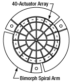
Click for Details
Diagram Showing Actuator Numbering and Layout for the DMP40 Mirrors
- 40-Actuator Array with 3 Bimorph Benders for ±2.0 mrad Tip/Tilt Actuation
- Ø10.0 mm Pupil, Ø11.5 mm Optical Aperture
- Two Metallic Mirror Coatings Available from Stock:
- UV-Enhanced Aluminum (250 nm - 450 nm)
- Protected Silver (450 nm - 20 µm)
- Single-Wavelength Crystalline Coatings Available for 900 nm to 5.0 µm via Tech Support
Our DMP40 series piezoelectric deformable mirrors are each comprised of 40 independently controlled actuators with either a UV-enhanced aluminum or protected silver reflective coating. The mirror includes three spiral bimorph bender arms which enable tip/tilt actuation of the coated surface.
| Physical Strokea | |||||||
|---|---|---|---|---|---|---|---|
| Aberration | Defocus | Astigmatism | Coma | Trefoil | Tetrafoil | Secondary Astigmatism |
Third Order Spherical Aberation |
| Zernike Coefficient | Z5 | Z4, Z6 | Z8, Z9 | Z7, Z10 | Z11, Z15 | Z12, Z14 | Z13 |
| Value | ±6.5 µmb | ±6.8 µmb | ±2.5 µmb | ±2.4 µmb | ±2.1 µmb | ±1.1 µmb | ±1.0 µmb |

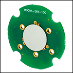
Click to Enlarge
The internal circuit board and mirror of a DMH series deformable mirrors.
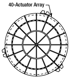
Click for Details
Diagram Showing Actuator Numbering and Layout for the DMH40 Mirrors
- 40-Actuator Array
- Ø14.0 mm Pupil, Ø17.0 mm Optical Aperture
- Two Metallic Mirror Coatings Available from Stock:
- UV-Enhanced Aluminum (250 nm - 450 nm)
- Protected Silver (450 nm - 20 µm)
- Single-Wavelength Crystalline Coatings Available for 900 nm to 5.0 µm via Tech Support
Our DMH40 series piezoelectric deformable mirrors are each comprised of 40 independently controlled actuators with a protected silver reflective coating. The mirror has a Ø14 mm pupil and a large actuator physical stroke as compared to the DMP40 series above. Note that this mirror does not have biomorph benders for tip/tilt actuation.
| Physical Strokea | |||||||
|---|---|---|---|---|---|---|---|
| Aberration | Defocus | Astigmatism | Coma | Trefoil | Tetrafoil | Secondary Astigmatism |
Third Order Spherical Aberration |
| Zernike Coefficient | Z5 | Z4, Z6 | Z8, Z9 | Z7, Z10 | Z11, Z15 | Z12, Z14 | Z13 |
| Value | ±17.6 µmb | ±18.4 µmb | ±6.8 µmb | ±6.5 µmb | ±5.7 µmb | ±3.0 µmb | ±2.7 µmb |
 Products Home


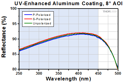
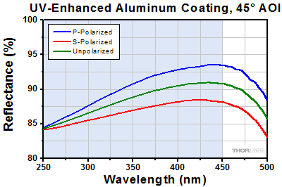
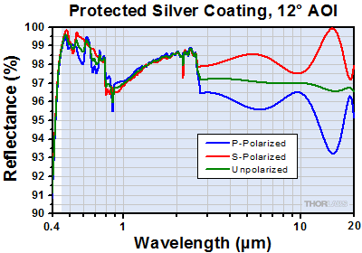
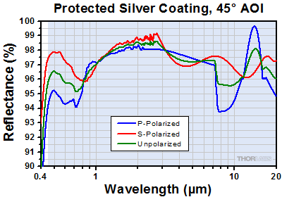

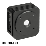
 Zoom
Zoom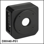
 Piezoelectric Deformable Mirrors